TIDUF71 March   2024


  1.   1
  2.   Description
  3.   Resources
  4.   Features
  5.   Applications
  6.   6
  7. 1System Description
  8. 2System Overview
    1. 2.1 Block Diagram
    2. 2.2 Design Considerations
    3. 2.3 Highlighted Products
      1. 2.3.1 AFE7950-SP
      2. 2.3.2 LMK04832-SEP
      3. 2.3.3 LMX2694-SEP
      4. 2.3.4 TPS7H4003-SEP
      5. 2.3.5 TPS7H4010-SEP
      6. 2.3.6 TPS73801-SEP
  9. 3Hardware, Software, Testing Requirements, and Test Results
    1. 3.1 Hardware Requirements
    2. 3.2 Software Requirements
    3. 3.3 Test Setup
    4. 3.4 Hardware Configuration
    5. 3.5 Test Procedure
      1. 3.5.1 Initial TSW14J56 Setup
      2. 3.5.2 Reference Design Test Procedure
    6. 3.6 Test Results
      1. 3.6.1 TXA/B DAC Output Test Results
      2. 3.6.2 TXC/D DAC Output Test Results
      3. 3.6.3 RXA/B ADC Test Results
      4. 3.6.4 RXC/D ADC Test Results
      5. 3.6.5 FB2 ADC Test Results
    7. 3.7 Alternative Configurations
      1. 3.7.1 Internal AFE7950-SP PLL/VCO
        1. 3.7.1.1 The Easy Way - Internal PLL/VCO
        2. 3.7.1.2 The Proper Way - Internal PLL/VCO
      2. 3.7.2 Internal TCXO Operation
      3. 3.7.3 400MHz Bandwidth RX Configuration
  10. 4Design and Documentation Support
    1. 4.1 Design Files
      1. 4.1.1 Schematics
      2. 4.1.2 BOM
    2. 4.2 Tools and Software
      1. 4.2.1 Latte Commands
      2. 4.2.2 Config Files
        1. 4.2.2.1 Latte Config Files
        2. 4.2.2.2 LMK / LMX Config Files
      3. 4.2.3 Troubleshooting
    3. 4.3 Hardware Identification Information
      1. 4.3.1 Rework Modifications
      2. 4.3.2 Reference Design Board Location Identification
      3. 4.3.3 FMC Interface Board Location Identification
    4. 4.4 Documentation Support
    5. 4.5 Support Resources
    6. 4.6 Trademarks
  11. 5About the Author

TXA/B DAC Output Test Results

The config file is setup on channels TXA and TXB with the NCO set to 2.1GHz. The TSW14J56 is setup with a tone at 10MHz offset. Expect the output tone at about 2110MHz. Note, the offset is not exactly 10MHz due to the multi-tone set-up. Figure 3-3 shows the output tone performance.

The spur at 1MHz offset is from the 1.2V, 1.8V, and 3.3V DC-DC switchers. The 1.2V supply couples most prominently to the external clock due to the proximity.

The output power is approximately 4dBm. Note, the config file engages a 10dB attenuator on the AFE7950-SP to maintain that the TRF0208 device is not over-driven.
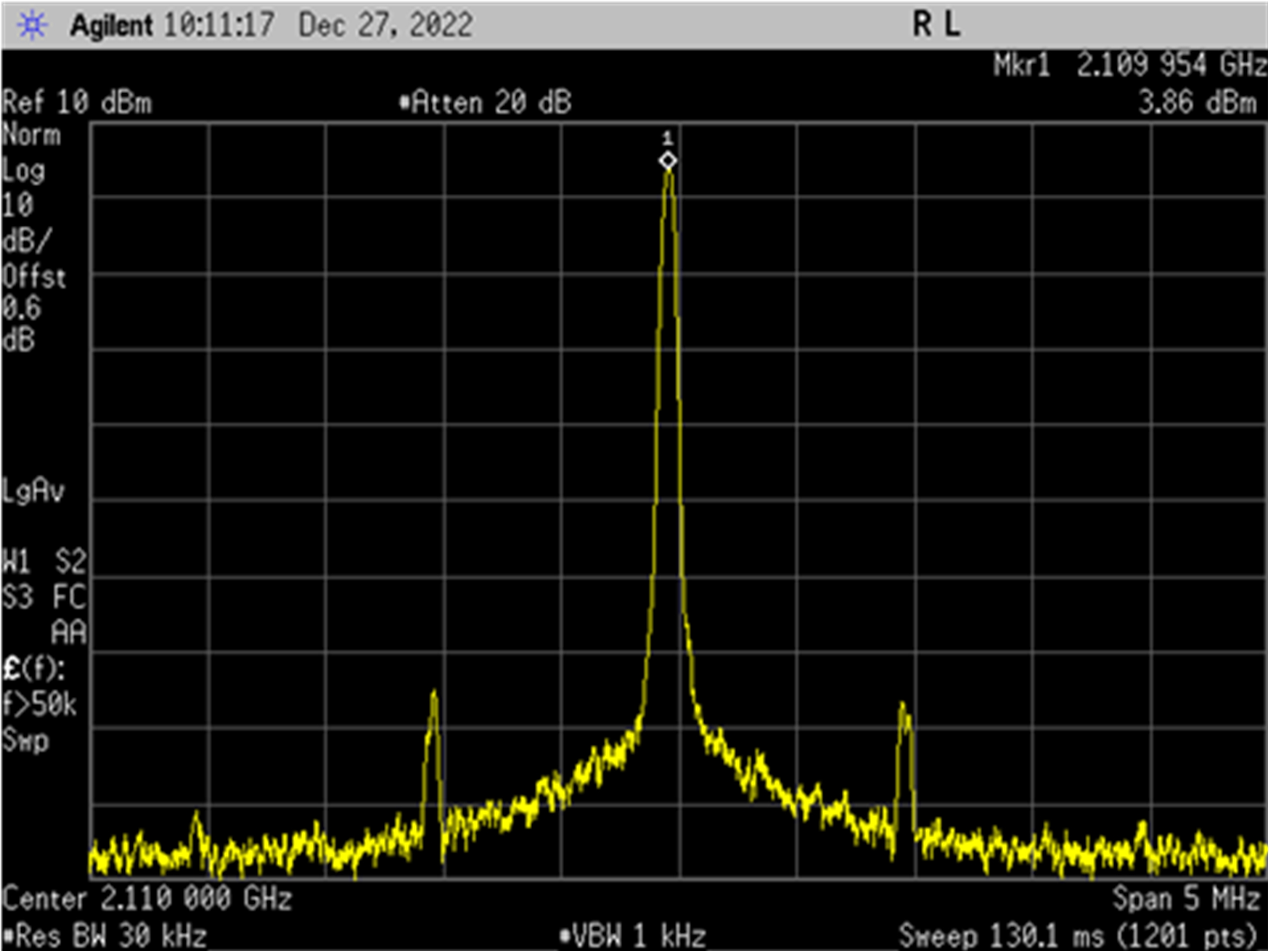
GUID-20240123-SS0I-4TQJ-NDPF-BBRLGXZNJ9LT-low.jpg Figure 3-3 TXA/B DAC Output Performance