TIDUF71A
March 2024 – November 2024
1
Description
Resources
Features
Applications
6
1
System Description
2
System Overview
2.1
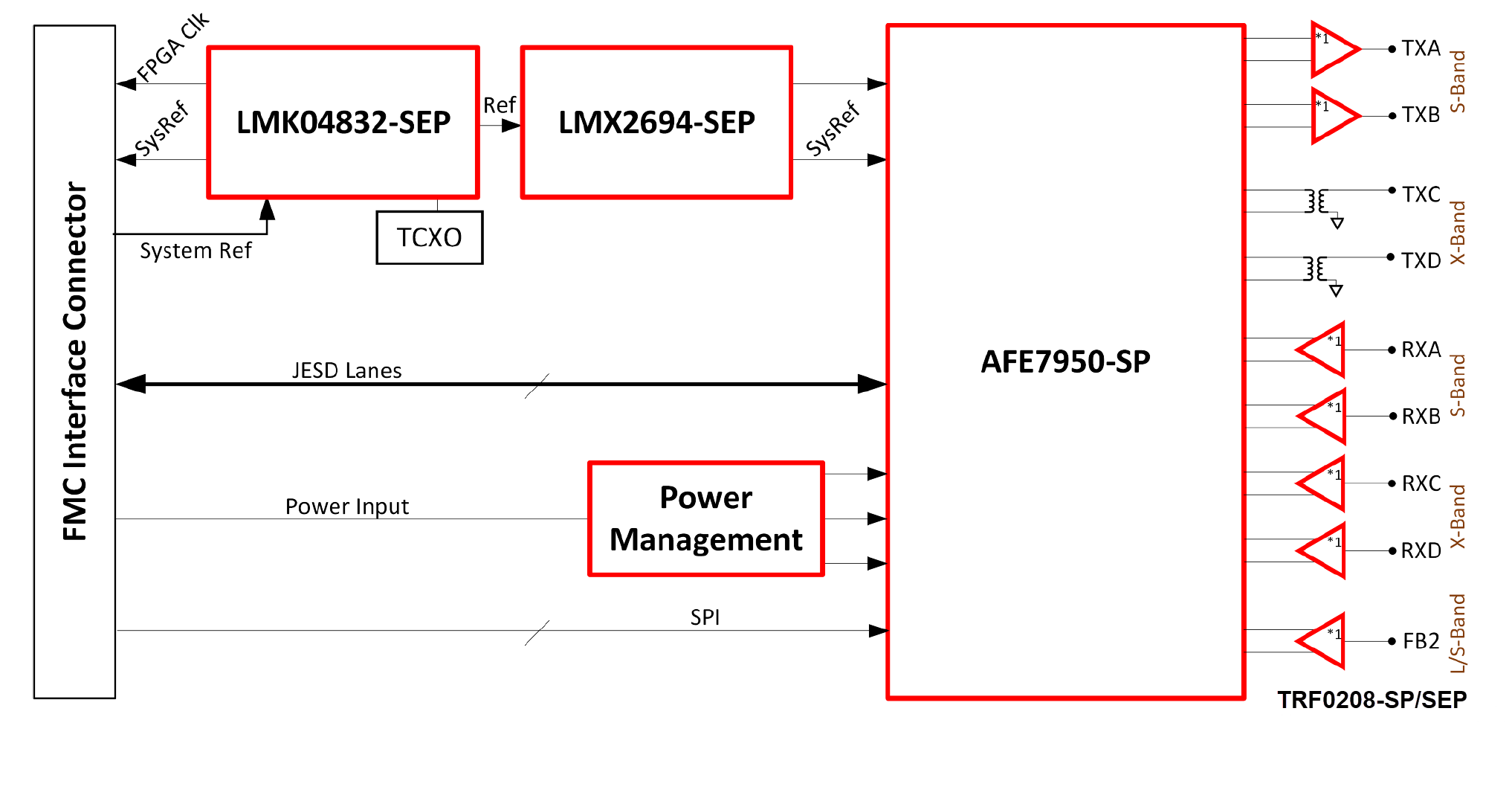
Block Diagram
2.2
Design Considerations
2.3
Highlighted Products
2.3.1
AFE7950-SP
2.3.2
LMK04832-SEP
2.3.3
LMX2694-SEP
2.3.4
TRF0208-SEP
2.3.5
TPS7H4010-SEP
2.3.6
TPS73801-SEP
3
Hardware, Software, Testing Requirements, and Test Results
3.1
Hardware Requirements
3.2
Software Requirements
3.3
Test Setup
3.4
Hardware Configuration
3.5
Test Procedure
3.5.1
Initial TSW14J56 Setup
3.5.2
Reference Design Test Procedure
3.6
Test Results
3.6.1
TXA/B DAC Output Test Results
3.6.2
TXC/D DAC Output Test Results
3.6.3
RXA/B ADC Test Results
3.6.4
RXC/D ADC Test Results
3.6.5
FB2 ADC Test Results
3.7
Alternative Configurations
3.7.1
Internal AFE7950-SP PLL/VCO
3.7.1.1
The Easy Way - Internal PLL/VCO
3.7.1.2
The Proper Way - Internal PLL/VCO
3.7.2
Internal TCXO Operation
3.7.3
400MHz Bandwidth RX Configuration
4
Design and Documentation Support
4.1
Design Files
4.1.1
Schematics
4.1.2
BOM
4.2
Tools
4.2.1
Latte Commands
4.2.2
Config Files
4.2.2.1
Latte Config Files
4.2.2.2
LMK / LMX Config Files
4.2.3
Troubleshooting
4.3
Hardware Identification Information
4.3.1
Rework Modifications
4.3.2
Reference Design Board Location Identification
4.3.3
FMC Interface Board Location Identification
4.4
Documentation Support
4.5
Support Resources
4.6
Trademarks
5
About the Author
6
Revision History