TIDUF71A March   2024  – November 2024


  1.   1
  2.   Description
  3.   Resources
  4.   Features
  5.   Applications
  6.   6
  7. 1System Description
  8. 2System Overview
    1. 2.1 Block Diagram
    2. 2.2 Design Considerations
    3. 2.3 Highlighted Products
      1. 2.3.1 AFE7950-SP
      2. 2.3.2 LMK04832-SEP
      3. 2.3.3 LMX2694-SEP
      4. 2.3.4 TRF0208-SEP
      5. 2.3.5 TPS7H4010-SEP
      6. 2.3.6 TPS73801-SEP
  9. 3Hardware, Software, Testing Requirements, and Test Results
    1. 3.1 Hardware Requirements
    2. 3.2 Software Requirements
    3. 3.3 Test Setup
    4. 3.4 Hardware Configuration
    5. 3.5 Test Procedure
      1. 3.5.1 Initial TSW14J56 Setup
      2. 3.5.2 Reference Design Test Procedure
    6. 3.6 Test Results
      1. 3.6.1 TXA/B DAC Output Test Results
      2. 3.6.2 TXC/D DAC Output Test Results
      3. 3.6.3 RXA/B ADC Test Results
      4. 3.6.4 RXC/D ADC Test Results
      5. 3.6.5 FB2 ADC Test Results
    7. 3.7 Alternative Configurations
      1. 3.7.1 Internal AFE7950-SP PLL/VCO
        1. 3.7.1.1 The Easy Way - Internal PLL/VCO
        2. 3.7.1.2 The Proper Way - Internal PLL/VCO
      2. 3.7.2 Internal TCXO Operation
      3. 3.7.3 400MHz Bandwidth RX Configuration
  10. 4Design and Documentation Support
    1. 4.1 Design Files
      1. 4.1.1 Schematics
      2. 4.1.2 BOM
    2. 4.2 Tools
      1. 4.2.1 Latte Commands
      2. 4.2.2 Config Files
        1. 4.2.2.1 Latte Config Files
        2. 4.2.2.2 LMK / LMX Config Files
      3. 4.2.3 Troubleshooting
    3. 4.3 Hardware Identification Information
      1. 4.3.1 Rework Modifications
      2. 4.3.2 Reference Design Board Location Identification
      3. 4.3.3 FMC Interface Board Location Identification
    4. 4.4 Documentation Support
    5. 4.5 Support Resources
    6. 4.6 Trademarks
  11. 5About the Author
  12. 6Revision History

Internal TCXO Operation

The default test procedure outlines uses an external high-quality reference oscillator at 491.52MHz which is buffered or divided by the LMK04832-SEP in bypass mode. Alternatively, the reference design has an on-board 30.72MHz TCXO. This TCXO can serve as the reference for the LMK internal PLL/VCO. With this approach, the internal PLL/VCO is locked to 2949.12MHz. That output signal is divided down to supply the necessary clocks to the AFE, LMX, and FPGA.

Implement this approach by executing the following config file during the bring-up of the LMK04832:

  • LMK04832-SEP: LMK04832-SEP_TICsPro_2949p12M_VCO_30p72_TCXO.tcs

The disadvantage of this approach is the degraded phase noise performance of the AFE reference signal that is derived from the LMK VCO compared to a high quality TCXO like a Wenzel Oscillator. Figure 3-9 shows performance of the AFE7950-SP with internal PLL/VCO clock where the reference is derived from the LMK VCO.
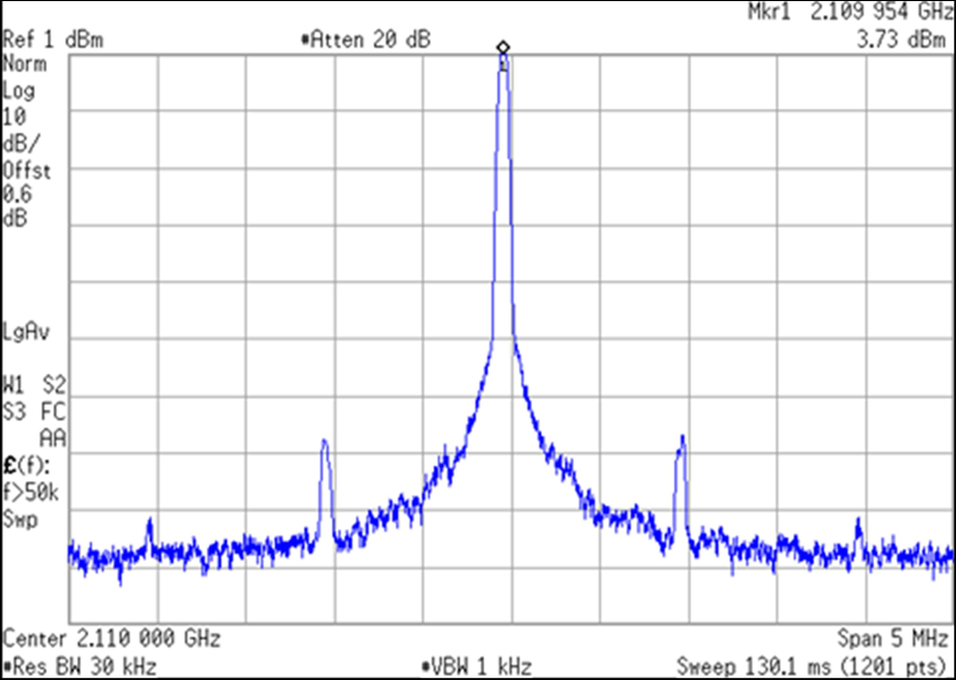
TIDA-010260 TXA Output With LMX Reference
                    Derived From TCXO Figure 3-9 TXA Output With LMX Reference Derived From TCXO