TIDUF72 August 2024
- 1
- Description
- Resources
- Features
- Applications
- 6
- 1System Description
- 2System Overview
-
3Hardware, Software, Testing Requirements, and Test Results
- 3.1
Hardware Requirements
- 3.1.1 Software Requirements
- 3.1.2 UART for PC GUI Communication
- 3.1.3 Direct Memory Access (DMA)
- 3.1.4 ADC Setup
- 3.1.5 Foreground Process
- 3.1.6 Formulas
- 3.1.7 Background Process
- 3.1.8 Software Function per_sample_dsp()
- 3.1.9 Voltage and Current Signals
- 3.1.10 Pure Waveform Samples
- 3.1.11 Frequency Measurement and Cycle Tracking
- 3.1.12 LED Pulse Generation
- 3.1.13 Phase Compensation
- 3.2
Test Setup
- 3.2.1 Power Supply Options and Jumper Setting
- 3.2.2 Electricity Meter Metrology Accuracy Testing
- 3.2.3 Viewing Metrology Readings and Calibration
- 3.2.4 Calibration and FLASH Settings for MSPM0+ MCU
- 3.2.5 Gain Calibration
- 3.2.6 Voltage and Current Gain Calibration
- 3.2.7 Active Power Gain Calibration
- 3.2.8 Offset Calibration
- 3.2.9 Phase Calibration
- 3.3 Test Results
- 3.1
Hardware Requirements
- 4Design and Documentation Support
- 5About the Authors
3.2 Test Setup
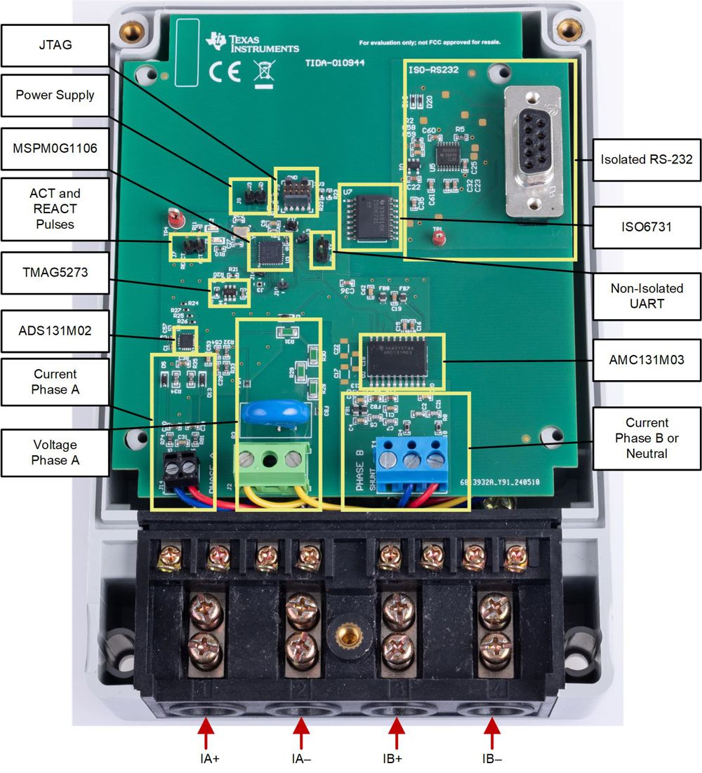
Top View of TIDA-010944 Design With Components Highlighted shows the TIDA-010944 photo with all functions on the top layer of the PCB; the bottom layer of the PCB has no components.
 Figure 3-9 Top View of TIDA-010944 Design
With Components Highlighted
Figure 3-9 Top View of TIDA-010944 Design
With Components HighlightedThe Phase A voltage is applied to J2, whereas terminal blocks J1 and J14 are used to connect the shunts for Phase B and A respectively.
Terminal blocks J2 has two positions: position 1 connects to Phase A voltage, whereas position 2 connects either to Neutral (single-phase star with 1P2W) or Phase B voltage (split-phase delta with 2 line voltages of 180° apart or 2P2W).