TIDUF73 September   2024


  1.   1
  2.   Description
  3.   Resources
  4.   Features
  5.   Applications
  6.   6
  7. 1System Description
  8. 2System Overview
    1. 2.1 Block Diagram
    2. 2.2 Design Considerations
      1. 2.2.1 Design Theory
      2. 2.2.2 Resistor Selection
        1. 2.2.2.1 Transistor and Diode Selection
      3. 2.2.3 Overcurrent Detection – Short-Circuit Protection
    3. 2.3 Highlighted Products
      1. 2.3.1 TPSI3100-Q1
      2. 2.3.2 INA180-Q1
      3. 2.3.3 TPSI2140-Q1
  9. 3Hardware, Software, Testing Requirements, and Test Results
    1. 3.1 Hardware Requirements
      1. 3.1.1 External Hardware Requirements
    2. 3.2 Test Setup
    3. 3.3 Test Results
  10. 4Design and Documentation Support
    1. 4.1 Design Files
      1. 4.1.1 Schematics
      2. 4.1.2 BOM
    2. 4.2 Tools
    3. 4.3 Documentation Support
    4. 4.4 Support Resources
    5. 4.5 Trademarks
  11. 5About the Author

Test Results

Figure 3-3 shows a typical precharge cycle and Figure 3-4 a discharge cycle.

  • VDRV is the drive pin on the secondary side of TPSI3100-Q1
  • VCAP is the voltage across the capacitor bank
  • EN_DSHCG is the enable signal for the TPSI2140-Q1
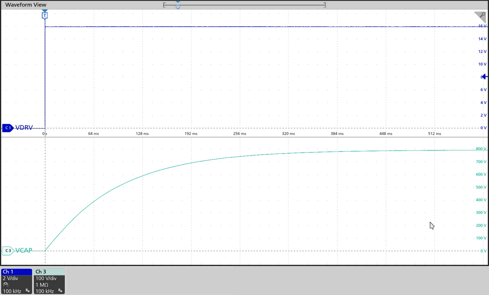
TIDA-050080 Precharge Cycle Figure 3-3 Precharge Cycle
TIDA-050080 Discharge Cycle Figure 3-4 Discharge Cycle

Figure 3-5 shows the VDRV pin disabling after the current has exceeded the 25A limit. After the auto-recovery period has passed, the drive pin re-asserts. Similarly, in Figure 3-6, the nFLT pin on the primary side reports the fault by pulling down after 30μs passes. This pin is pulled back up after another 30μs passes.
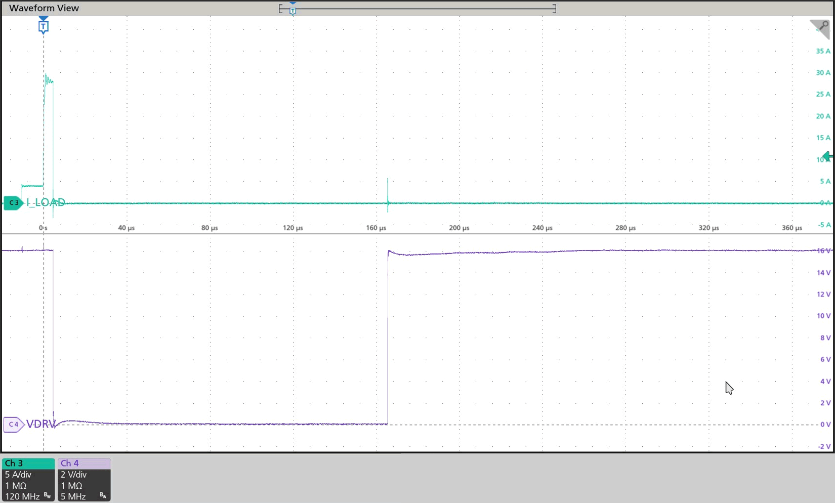
TIDA-050080 VDRV Disable and
                    Re-enable Figure 3-5 VDRV Disable and Re-enable
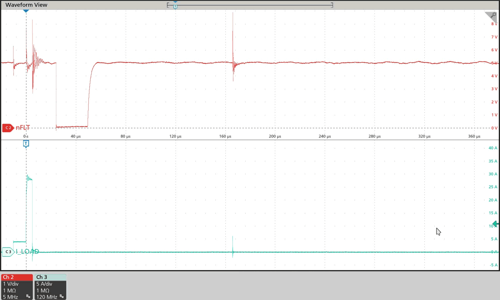
TIDA-050080 Primary Side Fault
                    Reporting Figure 3-6 Primary Side Fault Reporting