TIDUF78 May 2024
4.3.3 SPI Signal Measurement
Figure 4-14 shows the 32-bit SPI timing frame with nCS1 measured at the first TMAG5170 (U7) in the daisy-chain. The red signal is the SDI write frame (read command) and the corresponding special 32-bit SDO read frame with the two 12-bit X and Z field data, the status bits and the CRC. The transfer takes 3.4us.
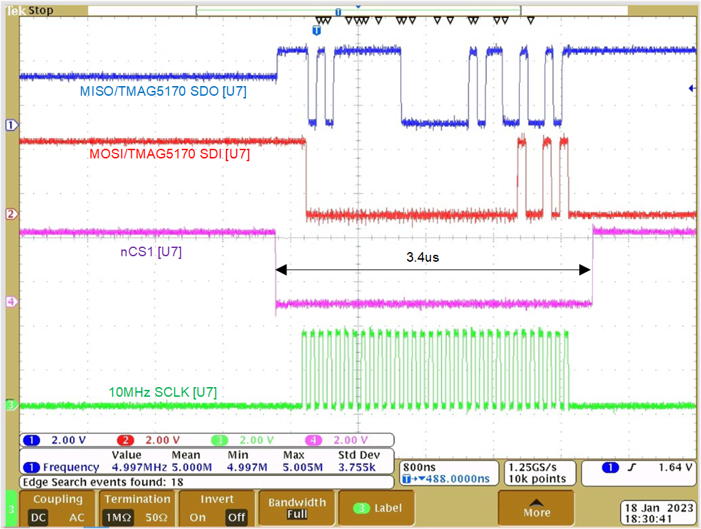 Figure 4-15 SPI 32-bit Frame
Timing
Figure 4-15 SPI 32-bit Frame
TimingFigure 4-15shows the timing of TMAG5170 (U7) SDO output versus the SPI clock SCLK input. The delay time of the SDO signal versus the falling clock edge is 20ns. The SDO rise time is 7ns, the fall time 3ns.
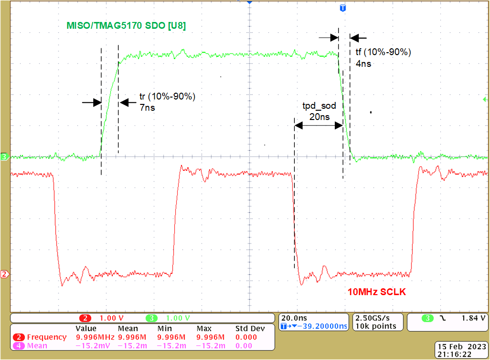 Figure 4-16 TMAG5170 U8 SDO (MISO) and
SCLK
Figure 4-16 TMAG5170 U8 SDO (MISO) and
SCLKFigure 4-16 shows the timing of SDO output versus the SPI clock SCLK input at the TIDA-060045 MCU headers J3-20 and J2-13. The setup time tsu is 22ns, the hold time th is 66ns versus the rising clock edge.
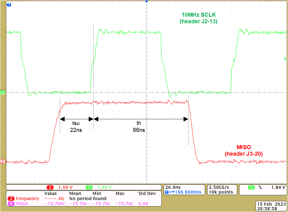 Figure 4-17 MISO and SCLK at MCU Headers
J2 and J3
Figure 4-17 MISO and SCLK at MCU Headers
J2 and J3Figure 4-17 shows the timing of TMAG5170 SDI input (MOSI) versus the 10MHz SPI clock (SCLK). Both the setup time (tsu_si=47ns) and hold time (th_si=48ns) meet the 25ns (MIN) TMAG5170 requirement.
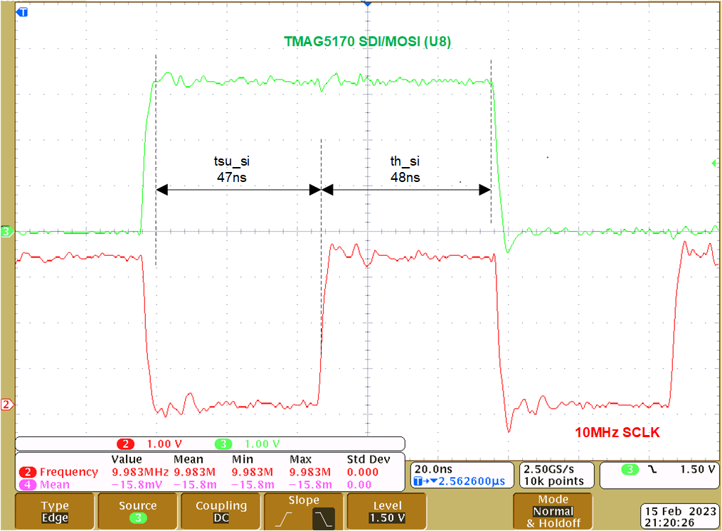 Figure 4-18 TMAG5170 U8 SDI (MOSI) and
SCLK
Figure 4-18 TMAG5170 U8 SDI (MOSI) and
SCLKThe following figures show a comparison of the SPI clock (SCLK) signal measured at the first TMAG5170 MCU (U7) and the last TMAG5170 (U8) in the SCLK daisy-chain with and without AC parallel termination.
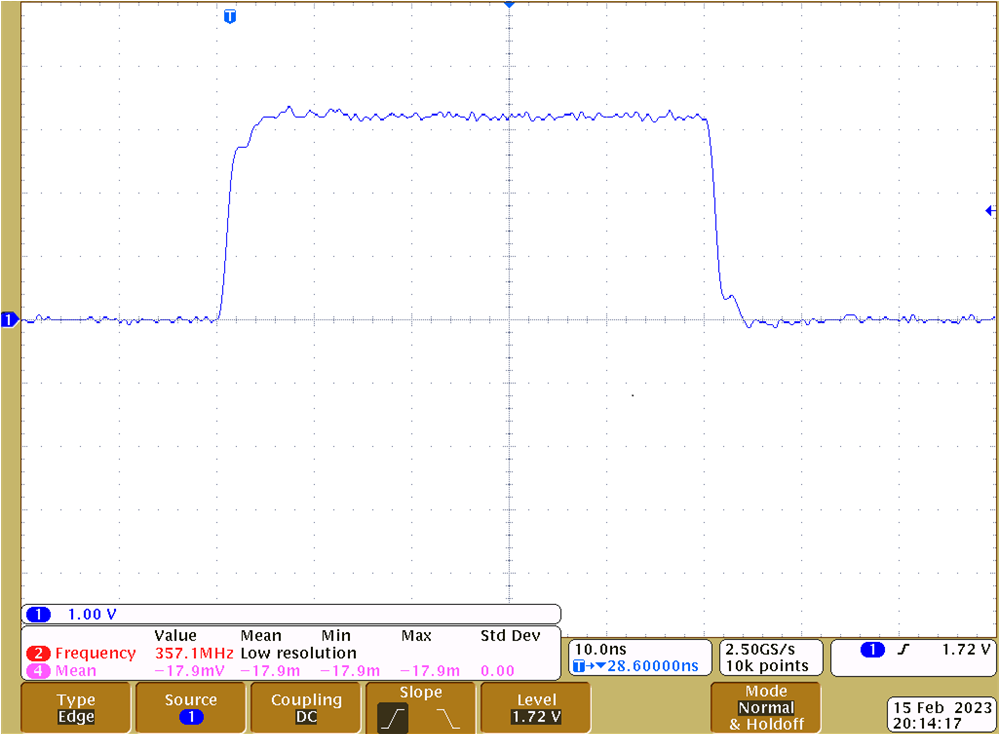 Figure 4-19 SCLK at U7 With AC Parallel
Termination at U8
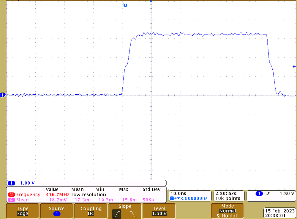 Figure 4-20 SCLK at U7 Without Parallel AC
Termination at U8
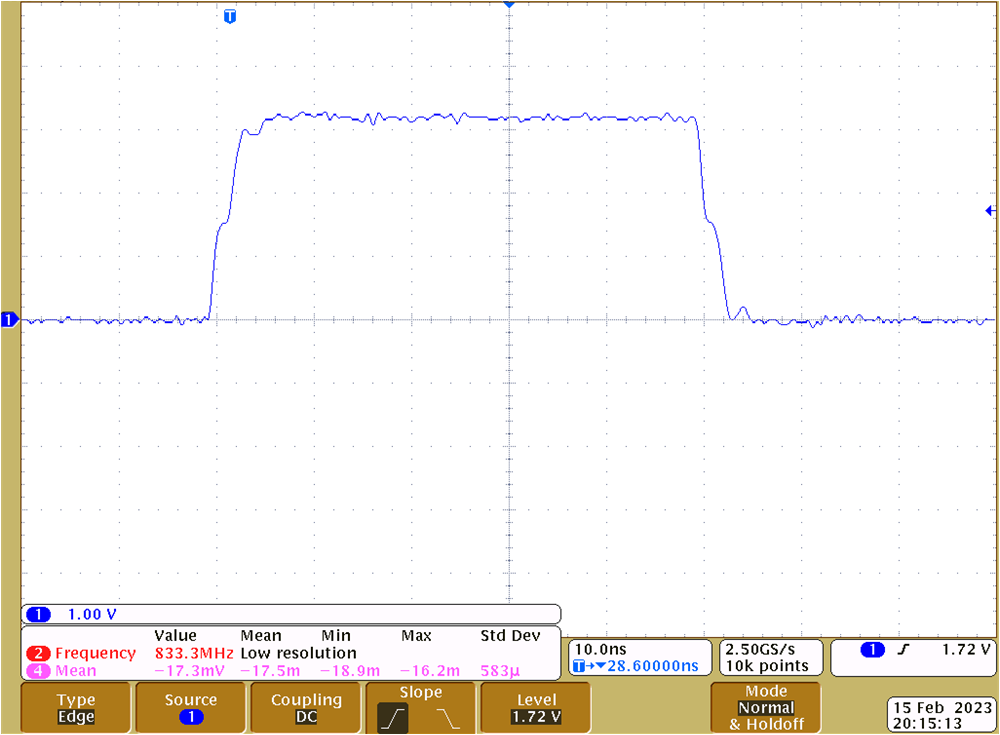 Figure 4-21 SCLK at U8 With AC Parallel
Termination at U8
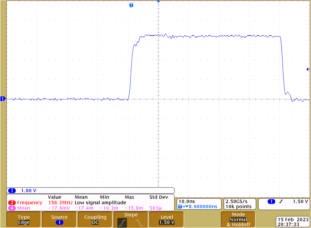 Figure 4-22 SCLK at U8 Without Parallel AC
Termination at U8
Figure 4-22 SCLK at U8 Without Parallel AC
Termination at U8The series line termination resistors for the MCU output signals nALERT, MOSI, SCLK and nCS1 to nCS4 have a 0Ω series line termination resistor close to the MCH header. The reason that these resistors are 0Ω by default is that the corresponding traces on the TMS320F280049C LaunchPad are similar length that on the TIDA-060045.
The SPI traces on the TIDA-060045 are less than 20cm (8 inch). The corresponding propagation delay of around 1.3ns is rather small versus the rise and fall-time. There was no significant impact of the AC parallel termination, when the F280049C LaunchPad was connected.
For custom designs, the series line termination resistors should be placed directly at the MCU’s output, which was not possible when using the TMS320F280049C LaunchPad. Depending on the SPI trace length AC parallel termination may be considered or not.