TIDUF87 November 2024
- 1
- Description
- Resources
- Features
- Applications
- 6
- 1System Description
- 2System Overview
-
3Hardware, Software, Testing Requirements, and Test Results
- 3.1 Hardware Requirements
- 3.2 Software Requirements
- 3.3 Test Setup
- 3.4
Test Procedure
- 3.4.1 Lab Variables Definitions
- 3.4.2 Lab 1. Open-Loop Current Control Single Phase
- 3.4.3 Lab 2. Closed Loop Current Control Single Phase
- 3.4.4 Lab 3. Open Loop Voltage Control Single Channel
- 3.4.5 Lab 4. Closed Loop Current and Voltage Control Single Channel
- 3.4.6 Lab 5. Closed Loop Current and Voltage Control Four Channels
- 3.4.7 Calibration
- 3.5 Test Results
- 4Design and Documentation Support
- 5About the Author
3.4.3.3 Running the Code
Use the following steps to run the code for Lab 2:
- To run this lab, make sure the hardware is set up as outlined in Section 3.3.2.
- Run the project by clicking
 from the menu bar.
 - In the watch view, check if the
BT4CH_InputVoltageSense_Vis from 12V to 15V in the Expression Window. - Set the following parameters from the Expression Window:
- Set the
BT4CH_userParam_chX->Relay_ONto 1 to enable the output relay. BT4CH_userParam_chX->iref_A= 15.0.- Set the
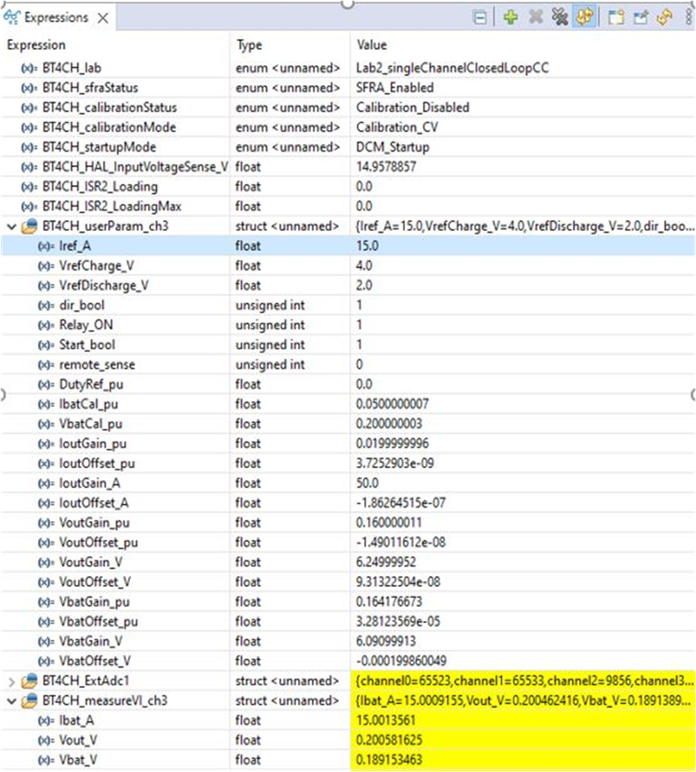
BT4CH_userParam_chX->en_bool= 1. - See Figure 3-19 for the Expression Window settings.
- Set the
- The
BT4CH_measureVI_chXvariable shows output current and voltage of the DC/DC converter. Isense1_A display value is close to iref_A setting with ±1mA error. - Figure 3-20 shows the SFRA setup to test the loop stability. Click on the Run SFRA icon from the SYSCONFIG page. The SFRA GUI pops up.
- Select the options for the device on the SFRA GUI; for example, for F28P65x, select Floating Point. Click on the Setup Connection button. In the pop-up window, uncheck the boot-on-connect option and select an appropriate COM port. Click the OK button. Return to the SFRA GUI and click the Connect button.
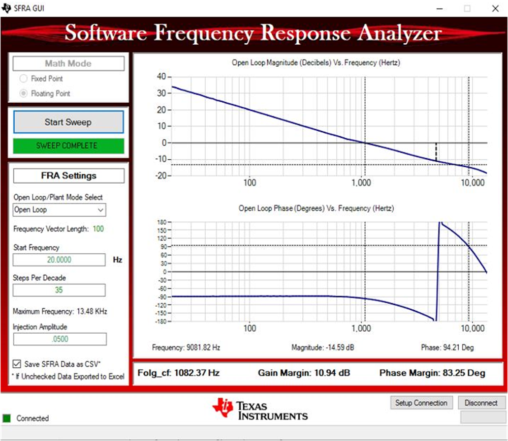
- The SFRA GUI connects to the device. A SFRA sweep can now be started by clicking Start Sweep. The complete SFRA sweep takes a few minutes to finish. Once complete, a graph with the measurement appears, as shown in Figure 3-21.
- The Frequency Response Data is saved in the project folder, under an SFRA Data folder, and is time-stamped with the time of the SFRA run.
 Figure 3-19 Lab 2 Expression Window, Closed Loop
 Figure 3-20 SFRA Setup for Closed-Loop Current Control
 Figure 3-21 Current Control Closed-Loop Frequency Response