TIDUF94 October   2024


  1.   1
  2.   Description
  3.   Resources
  4.   Features
  5.   Applications
  6.   6
  7. 1System Description
    1. 1.1 Key System Specifications
  8. 2System Overview
    1. 2.1 Block Diagram
    2. 2.2 Design Considerations
    3. 2.3 Highlighted Products
      1. 2.3.1 DP83TC818S-Q1 (Automotive SPE PHY)
      2. 2.3.2 TPS7B8233-Q1 (3.3V Vsleep Ultra-Low-IQ Low-Dropout Regulator)
      3. 2.3.3 TPS74701-Q1 (1.0V Rail Low-Dropout Regulator)
      4. 2.3.4 CDC6CE025000-Q1 (BAW Oscillator)
      5. 2.3.5 TPS4H160-Q1 (High-Side Switch)
  9. 3System Design Theory
    1. 3.1 Ethernet PHY
      1. 3.1.1 Ethernet PHY Power Supply
      2. 3.1.2 Ethernet PHY Clock Source
    2. 3.2 Power Coupling Network
      1. 3.2.1 High-Side Switch
  10. 4Hardware, Software, Testing Requirements, and Test Results
    1. 4.1 Hardware Requirements
    2. 4.2 Software Requirements
    3. 4.3 Test Setup
    4. 4.4 Test Results
  11. 5Design and Documentation Support
    1. 5.1 Design Files
      1. 5.1.1 Schematics
      2. 5.1.2 BOM
    2. 5.2 Tools and Software
    3. 5.3 Documentation Support
    4. 5.4 Support Resources
    5. 5.5 Trademarks
  12. 6About the Author

Ethernet PHY Power Supply

The DP83TC818S-Q1 is capable of operating with a wide range of I/O supply voltages (3.3V, 2.5V, or 1.8V). This board features an IO supply voltage of 3.3V to interface with various baseboards capable of 3.3V I/O voltage. The DP83TC818S-Q1 also requires a 1.0V rail. The implemented schematic shown in Figure 3-1 allows use of the DP83TC818S-Q1 integrated LDO to generate the required 1.0V. No power supply sequencing is required. Check and follow the DP83TC818S-Q1 Precise and Secure 100BASE-T1 Automotive Ethernet with TC10, IEEE802.1AS, IEEE802.1AE MACsec and AVB Clock Generation data sheet for the latest power supply device recommendation.
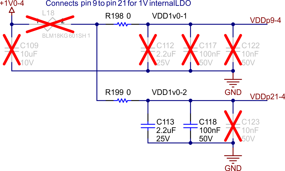
TIDA-020071 Ethernet PHY 1.0V Rail
                    Schematic Figure 3-1 Ethernet PHY 1.0V Rail Schematic