TIDUFA8 November   2024


  1.   1
  2.   Description
  3.   Resources
  4.   Features
  5.   Applications
  6.   6
  7. 1System Description
    1. 1.1 Terminology
    2. 1.2 Key System Specifications
  8. 2System Overview
    1. 2.1 Block Diagram
    2. 2.2 Highlighted Products
      1. 2.2.1 IWRL6432
    3. 2.3 Design Considerations
      1. 2.3.1 Reference Design Features
    4. 2.4 IWRL6432 Reference Design Architecture
      1. 2.4.1 IWRL6432: BOM Optimized Design
        1. 2.4.1.1 Device Power Topology
      2. 2.4.2 Power Distribution Network
      3. 2.4.3 Internal LDOs
        1. 2.4.3.1 Enabling and Disabling Low Power Mode
        2. 2.4.3.2 1.4V Power Supplies: APLL and Synthesizer
          1. 2.4.3.2.1 APLL 1.4V
          2. 2.4.3.2.2 SYNTHESIZER 1.4V
        3. 2.4.3.3 1.2V Power Supplies
          1. 2.4.3.3.1 RF 1.2V Supply
        4. 2.4.3.4 RF 1.0V Power Supply
      4. 2.4.4 Component Selection
        1. 2.4.4.1 1.8V DC-DC Regulator
          1. 2.4.4.1.1 Need for Forced PWM Mode Switching
          2. 2.4.4.1.2 Importance of Spread Spectrum Clocking
        2. 2.4.4.2 3.3V Low Dropout Regulator
        3. 2.4.4.3 FLASH Memory
        4. 2.4.4.4 Crystal
  9. 3System Design Theory
    1. 3.1 Antenna Specification
      1. 3.1.1 Antenna Requirements
      2. 3.1.2 Antenna Orientation
      3. 3.1.3 Bandwidth and Return Loss
      4. 3.1.4 Antenna Gain Plots
    2. 3.2 Antenna Array
      1. 3.2.1 2D Antenna Array With 3D Detection Capability
      2. 3.2.2 1D Antenna Array With 2D Detection Capability
    3. 3.3 PCB
      1. 3.3.1 Via-in-Pad Elimination
      2. 3.3.2 Micro-Via Process Elimination
    4. 3.4 Configuration Parameters
      1. 3.4.1 Antenna Geometry
      2. 3.4.2 Range and Phase Compensation
      3. 3.4.3 Chirp Configuration
    5. 3.5 Schematic and Layout Design Conditions
      1. 3.5.1 Internal LDO Output Decoupling Capacitor and Layout Conditions for BOM Optimized Topology
        1. 3.5.1.1 Single-Capacitor Rail
          1. 3.5.1.1.1 1.2V Digital LDO
        2. 3.5.1.2 Two-Capacitor Rail
          1. 3.5.1.2.1 1.2V RF LDO
        3. 3.5.1.3 1.2V SRAM LDO
        4. 3.5.1.4 1.0V RF LDO
      2. 3.5.2 Best and non-Best Layout Practices
        1. 3.5.2.1 Decoupling Capacitor Placement
        2. 3.5.2.2 Ground Return Path
        3. 3.5.2.3 Trace Width of High Current Carrying Traces
        4. 3.5.2.4 Ground Plane Split
  10. 4Link Budget
  11. 5Hardware, Software, Testing Requirements and Test Results
    1. 5.1 Hardware Requirements
      1. 5.1.1 Connection to the USB to UART Bridges
      2. 5.1.2 USB Cable to Connect to Host PC
      3. 5.1.3 The Rx-Tx Attribution of RS232
    2. 5.2 Software Requirements
    3. 5.3 Test Scenarios
    4. 5.4 Test Results
      1. 5.4.1 Human Detection at 15 Meters in Boresight
      2. 5.4.2 Antenna Radiation Plots
      3. 5.4.3 Angle Estimation Accuracy in Azimuth Plane
      4. 5.4.4 Angle Resolution
  12. 6Design and Documentation Support
    1. 6.1 Design Files
      1. 6.1.1 Schematics
      2. 6.1.2 BOM
      3. 6.1.3 PCB Layout Recommendations
        1. 6.1.3.1 Layout Prints
    2. 6.2 Tools and Software
    3. 6.3 Documentation Support
    4. 6.4 Support Resources
    5. 6.5 Trademarks
  13. 7About the Authors
SYNTHESIZER 1.4V

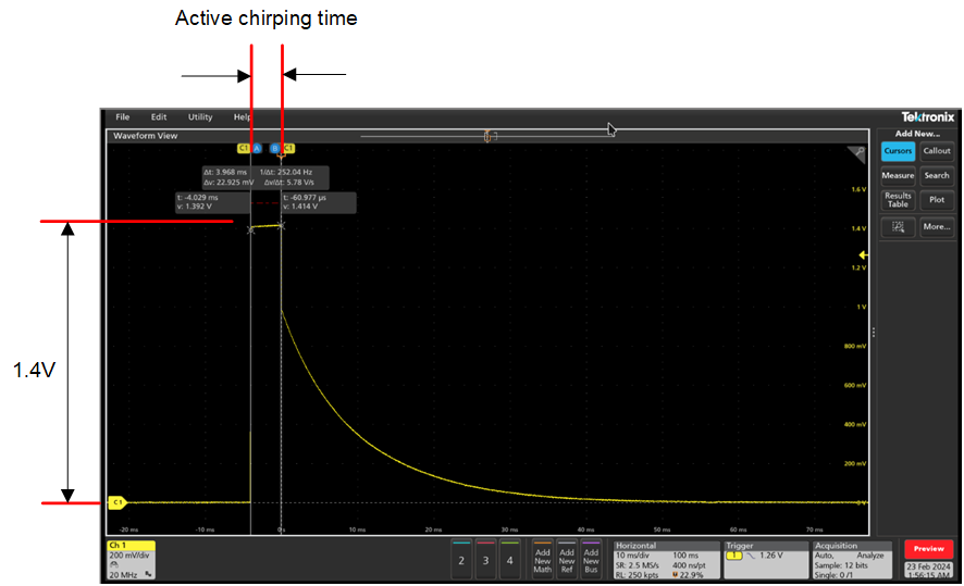
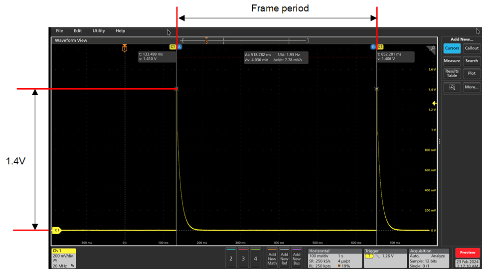
The 1.4V SYNTH supply stays at 0V after the device power up, until the device starts chirping. The supply rises to 1.4V sharply once chirping starts, and stays at the same voltage level until chirping ends in every frame. After that the supply drops to 0V until the next frame starts. Figure 2-13 and Figure 2-14 show the behavior of the 1.4V SYNTH supply.

Irrespective of low power mode, the synthesizer supply displays the same behavior.

TIDEP-01033 1.4V SYNTH - Wide
                    Window

Figure 2-13 1.4V SYNTH - Wide Window

TIDEP-01033 1.4V SYNTH - Close
                    Window

Figure 2-14 1.4V SYNTH - Close Window

The 1.4V SYNTH supply in low power operation, stays at 1.4V for the active chirp duration, 4ms for this case. After that the supply drops down to 0V until the next frame starts.