TIDUFA8 November   2024


  1.   1
  2.   Description
  3.   Resources
  4.   Features
  5.   Applications
  6.   6
  7. 1System Description
    1. 1.1 Terminology
    2. 1.2 Key System Specifications
  8. 2System Overview
    1. 2.1 Block Diagram
    2. 2.2 Highlighted Products
      1. 2.2.1 IWRL6432
    3. 2.3 Design Considerations
      1. 2.3.1 Reference Design Features
    4. 2.4 IWRL6432 Reference Design Architecture
      1. 2.4.1 IWRL6432: BOM Optimized Design
        1. 2.4.1.1 Device Power Topology
      2. 2.4.2 Power Distribution Network
      3. 2.4.3 Internal LDOs
        1. 2.4.3.1 Enabling and Disabling Low Power Mode
        2. 2.4.3.2 1.4V Power Supplies: APLL and Synthesizer
          1. 2.4.3.2.1 APLL 1.4V
          2. 2.4.3.2.2 SYNTHESIZER 1.4V
        3. 2.4.3.3 1.2V Power Supplies
          1. 2.4.3.3.1 RF 1.2V Supply
        4. 2.4.3.4 RF 1.0V Power Supply
      4. 2.4.4 Component Selection
        1. 2.4.4.1 1.8V DC-DC Regulator
          1. 2.4.4.1.1 Need for Forced PWM Mode Switching
          2. 2.4.4.1.2 Importance of Spread Spectrum Clocking
        2. 2.4.4.2 3.3V Low Dropout Regulator
        3. 2.4.4.3 FLASH Memory
        4. 2.4.4.4 Crystal
  9. 3System Design Theory
    1. 3.1 Antenna Specification
      1. 3.1.1 Antenna Requirements
      2. 3.1.2 Antenna Orientation
      3. 3.1.3 Bandwidth and Return Loss
      4. 3.1.4 Antenna Gain Plots
    2. 3.2 Antenna Array
      1. 3.2.1 2D Antenna Array With 3D Detection Capability
      2. 3.2.2 1D Antenna Array With 2D Detection Capability
    3. 3.3 PCB
      1. 3.3.1 Via-in-Pad Elimination
      2. 3.3.2 Micro-Via Process Elimination
    4. 3.4 Configuration Parameters
      1. 3.4.1 Antenna Geometry
      2. 3.4.2 Range and Phase Compensation
      3. 3.4.3 Chirp Configuration
    5. 3.5 Schematic and Layout Design Conditions
      1. 3.5.1 Internal LDO Output Decoupling Capacitor and Layout Conditions for BOM Optimized Topology
        1. 3.5.1.1 Single-Capacitor Rail
          1. 3.5.1.1.1 1.2V Digital LDO
        2. 3.5.1.2 Two-Capacitor Rail
          1. 3.5.1.2.1 1.2V RF LDO
        3. 3.5.1.3 1.2V SRAM LDO
        4. 3.5.1.4 1.0V RF LDO
      2. 3.5.2 Best and non-Best Layout Practices
        1. 3.5.2.1 Decoupling Capacitor Placement
        2. 3.5.2.2 Ground Return Path
        3. 3.5.2.3 Trace Width of High Current Carrying Traces
        4. 3.5.2.4 Ground Plane Split
  10. 4Link Budget
  11. 5Hardware, Software, Testing Requirements and Test Results
    1. 5.1 Hardware Requirements
      1. 5.1.1 Connection to the USB to UART Bridges
      2. 5.1.2 USB Cable to Connect to Host PC
      3. 5.1.3 The Rx-Tx Attribution of RS232
    2. 5.2 Software Requirements
    3. 5.3 Test Scenarios
    4. 5.4 Test Results
      1. 5.4.1 Human Detection at 15 Meters in Boresight
      2. 5.4.2 Antenna Radiation Plots
      3. 5.4.3 Angle Estimation Accuracy in Azimuth Plane
      4. 5.4.4 Angle Resolution
  12. 6Design and Documentation Support
    1. 6.1 Design Files
      1. 6.1.1 Schematics
      2. 6.1.2 BOM
      3. 6.1.3 PCB Layout Recommendations
        1. 6.1.3.1 Layout Prints
    2. 6.2 Tools and Software
    3. 6.3 Documentation Support
    4. 6.4 Support Resources
    5. 6.5 Trademarks
  13. 7About the Authors

Ground Return Path

The recommendation is to follow this design practice for all the on-chip LDO outputs to maintain shortest forward path.
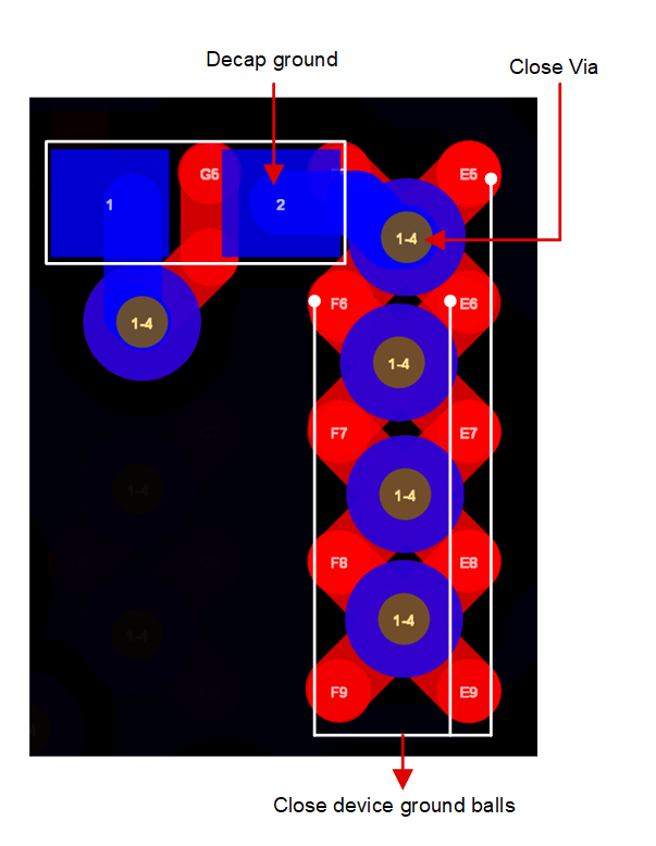

TIDEP-01033 Ground Return Path

Figure 3-31 Ground Return Path

An output path that can potentially act as a source of out-of-spec parasitic values consists of two elements:

  1. The forward path, that connects the BGA balls to the capacitor lead
  2. the ground return path that connects the capacitor ground to the device ground to close the loop. Figure 3-31 is a good example of ground return path.

As we can see in Figure 3-31, the decap ground is connected to a via which is placed very close to the ground lead of the capacitor. Further, the device ground is also very close to the via. This provides the shortest ground return path for the signal.