TIDUFA8 November 2024
- 1
- Description
- Resources
- Features
- Applications
- 6
- 1System Description
- 2System Overview
- 3System Design Theory
- 4Link Budget
- 5Hardware, Software, Testing Requirements and Test Results
- 6Design and Documentation Support
- 7About the Authors
3.5.1.2 Two-Capacitor Rail
1.2V RF LDO, 1.2V SRAM LDO and 1.0V RF LDO require two decoupling capacitors with typical values of 10uF and 2.2uF.

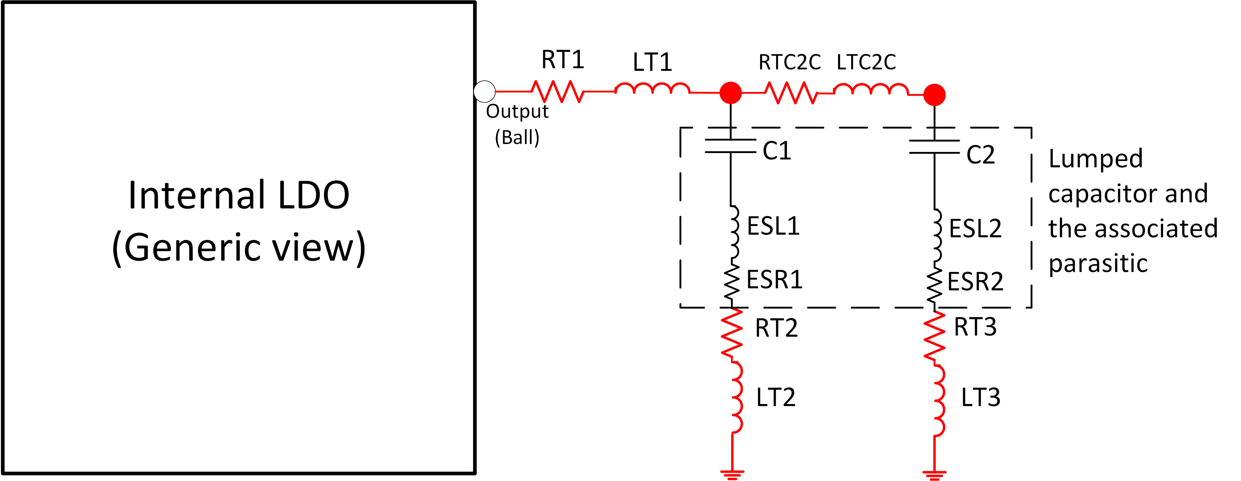
Figure 3-28 Parasitic Offered by Different Portion of the Output Path (for two Capacitors)
The parasitic offered by different portions of the output path is illustrated in Figure 3-28. As shown in the image, the output path can be divided into four portions:
- Ball to first capacitor:RT1 and LT1 are the parasitic resistance and inductance offered by the ball to the first capacitor lead.
- Along the first capacitor:ESL1 and ESR1 are the effective series inductance and resistance of the first decoupling capacitor. RT2 and LT2 are the ground trace resistance and inductance respectively of the first capacitor ground trace.
- First capacitor lead to second capacitor lead:RTC2C and LTC2C are the resistance and inductance of the trace between two capacitors.
- Along the second capacitor:ESL2 and ESR2 are the effective series inductance and resistance of the second decoupling capacitor. RT3 and LT3 are the ground trace resistance and inductance respectively of the second capacitor ground trace.
Note: Both the capacitors are recommended to be placed close to
the respective ball.