TIDUFA8 November   2024


  1.   1
  2.   Description
  3.   Resources
  4.   Features
  5.   Applications
  6.   6
  7. 1System Description
    1. 1.1 Terminology
    2. 1.2 Key System Specifications
  8. 2System Overview
    1. 2.1 Block Diagram
    2. 2.2 Highlighted Products
      1. 2.2.1 IWRL6432
    3. 2.3 Design Considerations
      1. 2.3.1 Reference Design Features
    4. 2.4 IWRL6432 Reference Design Architecture
      1. 2.4.1 IWRL6432: BOM Optimized Design
        1. 2.4.1.1 Device Power Topology
      2. 2.4.2 Power Distribution Network
      3. 2.4.3 Internal LDOs
        1. 2.4.3.1 Enabling and Disabling Low Power Mode
        2. 2.4.3.2 1.4V Power Supplies: APLL and Synthesizer
          1. 2.4.3.2.1 APLL 1.4V
          2. 2.4.3.2.2 SYNTHESIZER 1.4V
        3. 2.4.3.3 1.2V Power Supplies
          1. 2.4.3.3.1 RF 1.2V Supply
        4. 2.4.3.4 RF 1.0V Power Supply
      4. 2.4.4 Component Selection
        1. 2.4.4.1 1.8V DC-DC Regulator
          1. 2.4.4.1.1 Need for Forced PWM Mode Switching
          2. 2.4.4.1.2 Importance of Spread Spectrum Clocking
        2. 2.4.4.2 3.3V Low Dropout Regulator
        3. 2.4.4.3 FLASH Memory
        4. 2.4.4.4 Crystal
  9. 3System Design Theory
    1. 3.1 Antenna Specification
      1. 3.1.1 Antenna Requirements
      2. 3.1.2 Antenna Orientation
      3. 3.1.3 Bandwidth and Return Loss
      4. 3.1.4 Antenna Gain Plots
    2. 3.2 Antenna Array
      1. 3.2.1 2D Antenna Array With 3D Detection Capability
      2. 3.2.2 1D Antenna Array With 2D Detection Capability
    3. 3.3 PCB
      1. 3.3.1 Via-in-Pad Elimination
      2. 3.3.2 Micro-Via Process Elimination
    4. 3.4 Configuration Parameters
      1. 3.4.1 Antenna Geometry
      2. 3.4.2 Range and Phase Compensation
      3. 3.4.3 Chirp Configuration
    5. 3.5 Schematic and Layout Design Conditions
      1. 3.5.1 Internal LDO Output Decoupling Capacitor and Layout Conditions for BOM Optimized Topology
        1. 3.5.1.1 Single-Capacitor Rail
          1. 3.5.1.1.1 1.2V Digital LDO
        2. 3.5.1.2 Two-Capacitor Rail
          1. 3.5.1.2.1 1.2V RF LDO
        3. 3.5.1.3 1.2V SRAM LDO
        4. 3.5.1.4 1.0V RF LDO
      2. 3.5.2 Best and non-Best Layout Practices
        1. 3.5.2.1 Decoupling Capacitor Placement
        2. 3.5.2.2 Ground Return Path
        3. 3.5.2.3 Trace Width of High Current Carrying Traces
        4. 3.5.2.4 Ground Plane Split
  10. 4Link Budget
  11. 5Hardware, Software, Testing Requirements and Test Results
    1. 5.1 Hardware Requirements
      1. 5.1.1 Connection to the USB to UART Bridges
      2. 5.1.2 USB Cable to Connect to Host PC
      3. 5.1.3 The Rx-Tx Attribution of RS232
    2. 5.2 Software Requirements
    3. 5.3 Test Scenarios
    4. 5.4 Test Results
      1. 5.4.1 Human Detection at 15 Meters in Boresight
      2. 5.4.2 Antenna Radiation Plots
      3. 5.4.3 Angle Estimation Accuracy in Azimuth Plane
      4. 5.4.4 Angle Resolution
  12. 6Design and Documentation Support
    1. 6.1 Design Files
      1. 6.1.1 Schematics
      2. 6.1.2 BOM
      3. 6.1.3 PCB Layout Recommendations
        1. 6.1.3.1 Layout Prints
    2. 6.2 Tools and Software
    3. 6.3 Documentation Support
    4. 6.4 Support Resources
    5. 6.5 Trademarks
  13. 7About the Authors

Decoupling Capacitor Placement


TIDEP-01033 Decoupling Capacitor Placement: Non-Best Practice
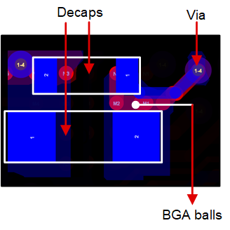
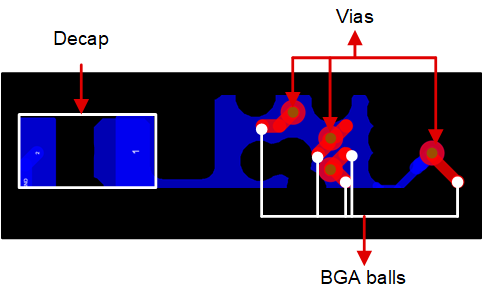
Figure 3-29 Decoupling Capacitor Placement: Non-Best Practice

TIDEP-01033 Decoupling Capacitor
                    Placement: Best Practice

Figure 3-30 Decoupling Capacitor Placement: Best Practice

On-chip LDOs require external capacitors for dominant pole compensation. For this, the capacitor placement and the output path traces become PCB design constraint dependent. The parasitic components contributed by the output path play a vital role in determining the system stability. In the previous section we have listed specific parasitic inductance and resistance values for each of the high bandwidth sensitive LDOs to make sure the stability of the power supplies. Here we are going to observe an example of good and bad practices while designing the PCB layout.

Figure 3-29 shows a design where the decap is placed far from the respective LDO-output BGA-balls. Considering the length of the complete trace connecting the balls to the capacitor lead by adding:

  1. The trace connecting the BGA balls to the respective vias in the top layer (traces marked in red are on the top layer of the PCB)
  2. Via length
  3. The trace connecting the vias to the capacitor lead (traces marked in blue are in the bottom layer of the PCB), we get a very long path. The combined parasitic of such long path can potentially alter the parasitic spec provided in data sheet, which can affect the LDO system stability.

Figure 3-30 shows a design where the capacitor is places very close to the BGA balls. Considering the possibilities of system instability involved with the previous example, this design is much better as the parasitic values are within the data sheet spec.