TIDUFA8 November 2024
- 1
- Description
- Resources
- Features
- Applications
- 6
- 1System Description
- 2System Overview
- 3System Design Theory
- 4Link Budget
- 5Hardware, Software, Testing Requirements and Test Results
- 6Design and Documentation Support
- 7About the Authors
2.4.1.1 Device Power Topology
The IWRL6432 can be operated in four different power topologies based on availability of the power supplies to the device with power consumption and BOM (cost) trade-off.
There are two topologies: power optimized topology and BOM optimized topology for IWRL6432. At most, three different supply voltages can be provided to the IWRL6432: 3.3V, 1.8V and 1.2V. The topologies are determined depending on whether the 1.2V is externally supplied to the device.
In power optimized topology, the 1.2V supply is externally provided. Higher current is provided by 1.2V rail which reduces the overall power consumption. This is why the topology is called power optimized. In BOM optimized topology, the 1.2V is NOT externally provided to the device. The on-chip LDOs generate the 1.2V supply there-by eliminating the need of external 1.2V rail. This is why this topology is called the BOM (bill of material) optimized topology.
The device supports two IO voltages: 3.3V and 1.8V. Thus, each of the power topologies can be further subdivided into two configurations depending on the IO voltage. At start-up, the device senses the number of external voltages provided and adjusts the IOs and determines whether the internal 1.2V supplies need to be activated. This creates incredible application based flexibility in terms of power topology and IO configuration.
The following tables summarize the power delivery to internal subsystems in different IO voltage operations under different topologies.
| Supply | Device Blocks Powered From the Supply |
|---|---|
| 3.3V | Digital I/Os |
| 1.8V | Synthesizer and APLL VCOs, crystal oscillator, IF Amplifier stages, ADC |
| 1.2V | Core Digital and SRAMs, RF, VNWA |
| SUPPLY | Device Blocks Powered From the Supply |
|---|---|
| 1.8V | Digital IOs, Synthesizer and APLL VCOs, crystal oscillator, IF Amplifier stages, ADC |
| 1.2V | Core Digital and SRAMs, RF, VNWA |
| SUPPLY | Device Blocks Powered From the Supply |
|---|---|
| 3.3V | Digital I/Os |
| 1.8V | Synthesizer and APLL VCOs, crystal oscillator, IF Amplifier stages, ADC |
| SUPPLY | Device Blocks Powered From the Supply |
|---|---|
| 1.8V | Digital IOs, Synthesizer and APLL VCOs, crystal oscillator, IF Amplifier stages, ADC |
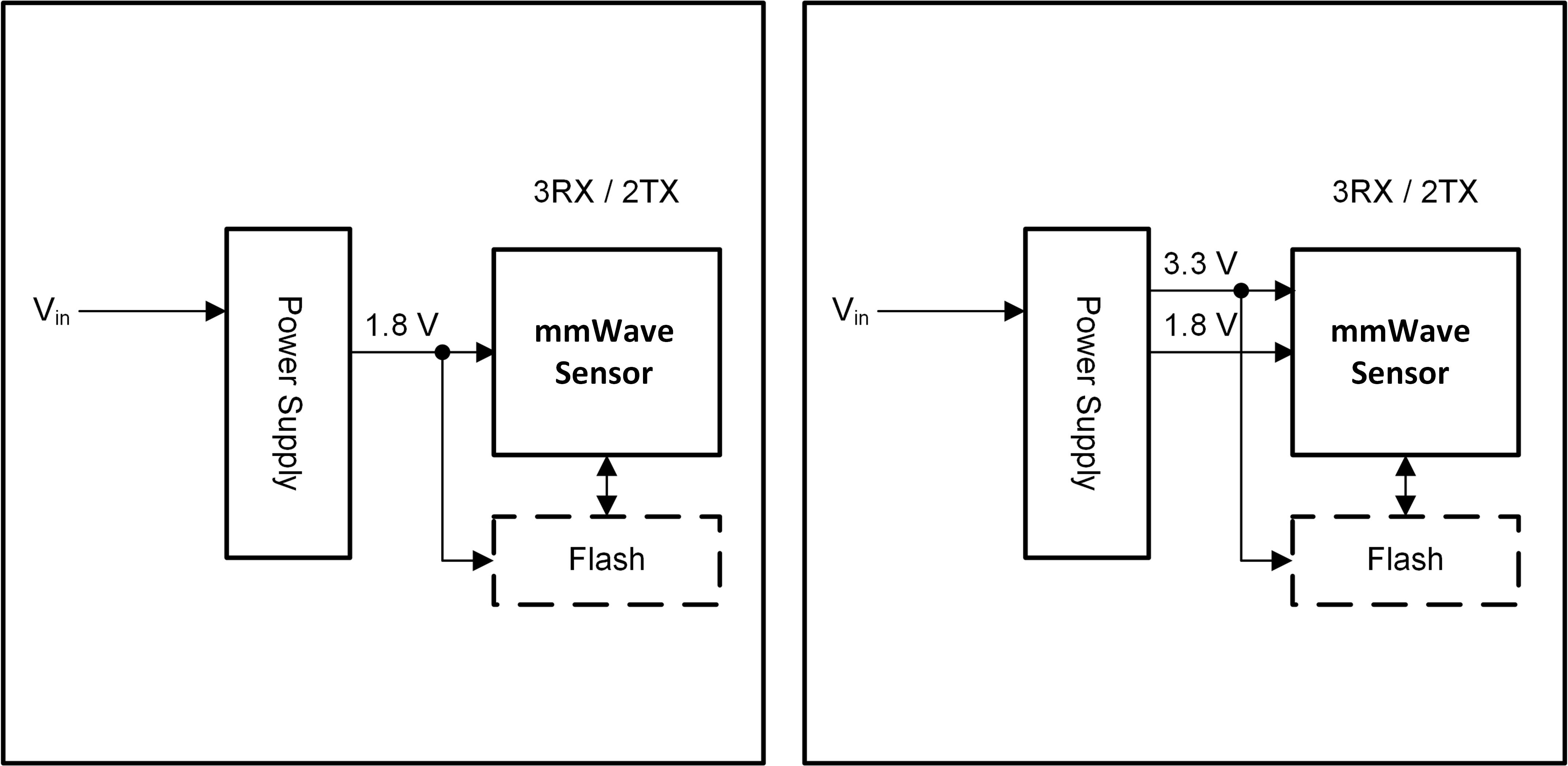
In BOM optimized mode, the device can be operated using one rail (1.8V) or two rails (3.3V and 1.8V) depending upon 1.8V IO or 3.3V IO respectively.
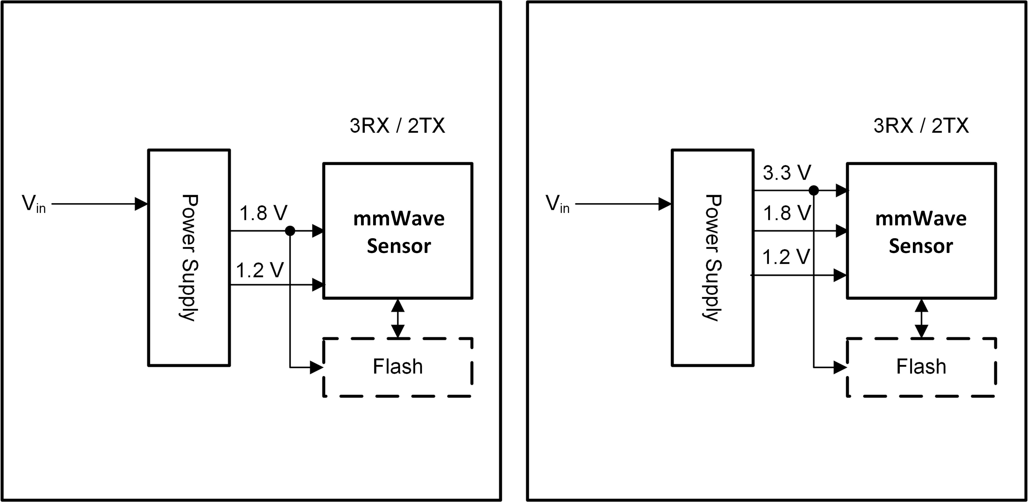
In power optimized mode, the device can either be powered using two rails (1.8V and 1.2V) or with three rails (3.3V, 1.8V and 1.2V). During initial boot up, the device senses whether the external 1.2V supply is present or not and based on that determines if internally generated 1.2V LDOs are needed. With the 1.2V rail externally provided, the on-chip LDOs are not enabled in this case.
 Figure 2-6 BOM Optimized Mode Power
Management (Left: Single Rail 1.8V I/O Topology, Right: Two Rails 3.3V I/O
Topology)
 Figure 2-7 Power Optimized Mode Power
Management (Left: Two Rails 1.8V I/O Topology, Right: Three Rails 3.3V I/O
Topology)
Figure 2-7 Power Optimized Mode Power
Management (Left: Two Rails 1.8V I/O Topology, Right: Three Rails 3.3V I/O
Topology)This reference design uses the BOM optimized topology (Figure 2-6) with provision to switch between 3.3V and 1.8V IO voltage operations.
The BOM optimized topology consumes little more power compared to that in the power optimized topology but optimizes the design cost significantly. Therefore, to optimize power consumption as well as cost, BOM optimized topology is used. For the power consumption comparison between different topologies, please refer to IWRL6432 Single-Chip 57- to 64GHz Industrial Radar Sensor, data sheet, section Typical Power Consumption Numbers.