TIDUFB8 December 2024
- 1
- Description
- Resources
- Features
- Applications
- 6
- 1System Description
- 2System Overview
- 3Hardware, Software, Testing Requirements, and Test Results
- 4Design and Documentation Support
- 5About the Author
3.3.1 Power Supply and Jumper Settings
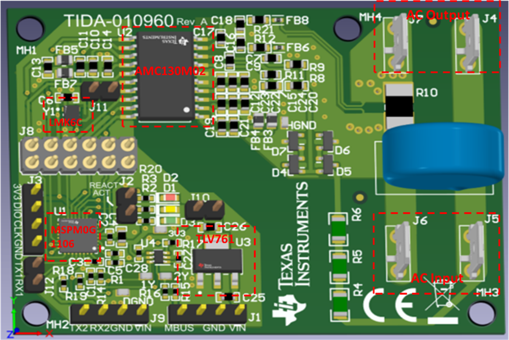
Figure 2-3 shows the location of various components of the reference design on the top layer of the PCB. The bottom layer has no soldered components.
 Figure 3-7 TIDA-010960 Hardware 3D
View
Figure 3-7 TIDA-010960 Hardware 3D
ViewTable 3-1 lists the jumper settings.
Table 3-1 Hardware Jumper Settings
| HEADER NAME |
TYPE | MAIN FUNCTIONALITY | COMMENTS |
|---|---|---|---|
| J1 | 4 pin | External power supply | Additional pin for M_BUS communication |
| J2 | 2 pin | Active and Reactive energy pulses | Those two pins are isolated from AC mains, but do not contain GND |
| J3 | 4 pin | JTAG: MSPM0 programming header | |
| J4, J7 | 1 pin | Positive and negative AC output header | Connect load the J4 J7 |
| J5, J6 | 1 pin | Positive and negative AC input header | Connect AC Line and Neutral to J5 J6 |
| J8 | 12 pin | Jumper to connect MSPM0 and AMC130M02 | Flexible setting for MCU |
| J9 | 4 pin | UART output to connect to main controller | |
| J10 | 2 pin | Jumper to connect 3.3V from external input power | |
| J11 | 2 pin | Jumper to connect clock from LMK6C to AMC1310M02 | Flexible setting for clock, LMK6C also connect to MSPM0 |
| J12 | 2 pin | UART to connect with PC GUI |