Circuit for driving high-voltage SAR ADCs for high-voltage, true differential signal acquisition
| Input | ADC Input | Digital Output ADS7042 |
|---|---|---|
| VinDiffMin = –20V | CH_x = +10V | 7FFFH, or 3276710 |
| VinDiffMax = +20V | CH_x = –10V | 8000H , or 3276810 |
| Power Supplies | |||
|---|---|---|---|
| AVDD | DVDD | VCC (HVDD) | VSS (HVSS) |
| 5.0V | 3.3V | +15V | –15V |
Design Description
This design shows a design to drive high-voltage SAR ADC to implement data capture for high-voltage fully differential signal which can have a wide common-mode voltage range depended on the power supply and input amplitude signal of the amplifier. A general high-voltage precision amplifier performs the differential to single-ended conversion and drives high-voltage SAR ADC single-ended input scale of ±10V at highest throughput. This type of application is popular in end equipment such as: Multi-Function Relays, AC Analog Input Modules, and Control Units for Rail Transport. The values in the component selection section can be adjusted to allow for different level differential input signal, different ADC data throughput rates, and different bandwidth amplifiers.
Specifications
| Specification | OPA827 Calculated | OPA827 Simulated | OPA192 Calculated | OPA192 Simulated |
|---|---|---|---|---|
| Common Mode Input Range (with Vdif = ±20V) | ±26V | ±26V | ±35V | ±35V |
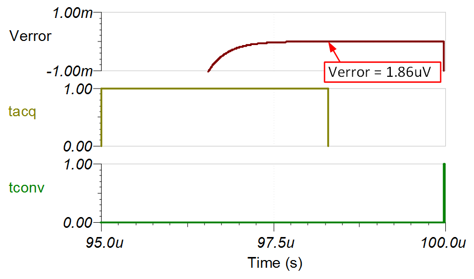
| Transient ADC Input Settling Error | < 1/2LSB (< 152µV) | 0.002 LSB (0.568µV) | < 1/2LSB (< 152µV) | 0.006 LSB (1.86µV) |
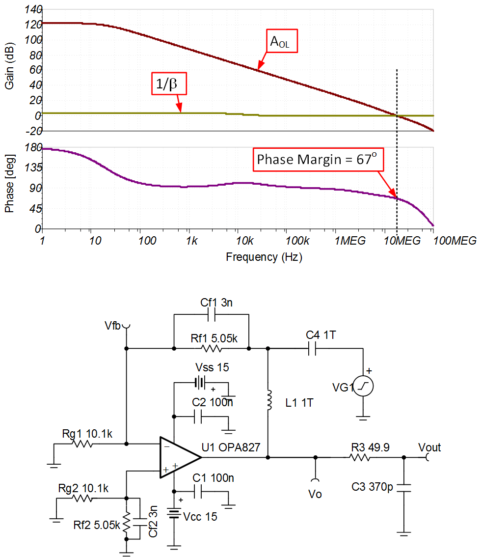
| Phase Margin of driver | > 45° | 67.1° | > 45° | 68.6° |
| Noise (at ADC Input) | 14.128µVrms | 15.88µVrms | 5.699µVrms | 6.44µVrms |
Design Notes
- Determine the amplifier gain based on the differential input signal level, the ADC’s configuration for input range. This is covered in the component selection section.
- Determine amplifier’s linear range based on common mode voltage, input swing, and power supplies. This is covered in the component selection section.
- In this design circuit, the common-mode voltage of the input signal can be any value in the range of VInputCM . The derivation of this range is provided in the component selection section for the OPA827 and OPA192.
- Select COG capacitors to minimize distortion.
- Use 0.1% 20ppm/°C film resistors or better for good accuracy, low gain drift, and to minimize distortion. Review Statistics Behind Error Analysis for methods to minimize gain, offset, drift, and noise errors.
- Refer to Introduction to SAR ADC Front-End Component Selection for an explanation of how to select Rfilt and Cfilt for best settling and AC performance. These component values are dependent on the amplifier bandwidth, data converter sampling rate, and data converter design. The values shown here provide good settling and AC performance for the amplifier and data converter in this example. If the design is modified, select a different RC filter.
Component Selection
- Find the gain based on differential
input signal and ADC full-scale input range.
- Find standard resistor values for
differential gain. Use the Analog Engineer's Calculator ("Amplifier and
Comparator\Find Amplifier Gain" section) to find standard values for Rf/Rg
ratio.
- Find the amplifier’s maximum and
minimum input for linear operation (that is, the common mode range of the
amplifier, Vcm_amp). For this example, the OPA827 is used.
- Calculate the maximum common-mode
voltage range based on the input range and previously shown configuration of the
amplifier. Refer to the schematic diagram on the first page for better
understanding of how Vcm_opa, VInputCM, and
Vdif relate to the circuit.
- Solve the equation for the input
common-mode range VInputCM for the amplifier. For this example
(OPA827), the common mode input can be ±26V with a ±20-V differential input.
Using the same method on OPA192 shows a common mode range of ±35V with a ±20-V
differential input. Exceeding this common-mode range distorts the signal. Note
that this common-mode range was calculated using ±15-V power supplies. The
common mode range can be extended by increasing the supply (maximum ±18V).
- Find the value for Cf that achieves
the desired closed-loop bandwidth. In this example, users need a 10kHz
bandwidth. Note: if users adjust the bandwidth, then users need to verify the
charge bucket filter settling (Cfilt and Rfilt) as the
closed-loop bandwidth effects settling.
- Find the value for Cfilt and Rfilt using TINA SPICE and the methods described in Introduction to SAR ADC Front-End Component Selection. The value of Rfilt and Cfilt shown in this document works for these circuits; however, if users use different amplifiers or different gain settings, then users must use TINA SPICE to find new values.
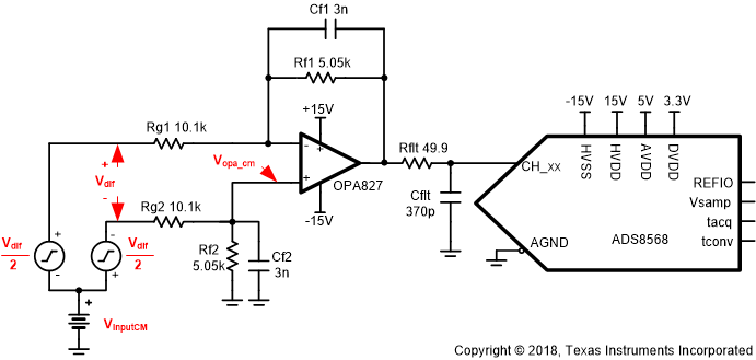
DC Transfer Characteristics
The following graph shows a linear output response for inputs from differential –20V to +20V. The full-scale range (FSR) of the ADC falls within the linear range of the op amp. Refer to Determining a SAR ADC's Linear Range when using Operational Amplifiers for detailed theory on this subject.
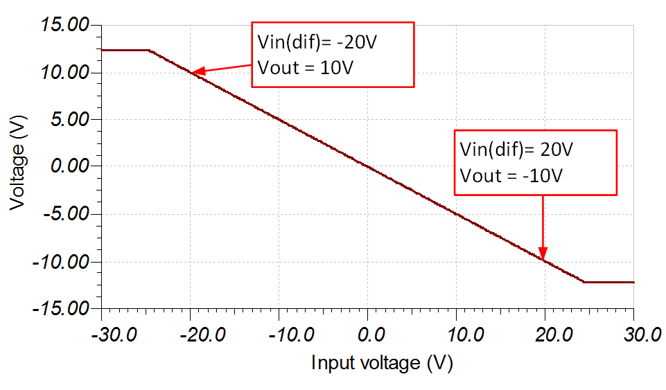
AC Transfer Characteristics
The bandwidth is simulated to be 10.58kHz and the gain is –6.038dB which is a linear gain of 0.5V/V. See the Op Amps: Bandwidth 1 video for more details on this subject.
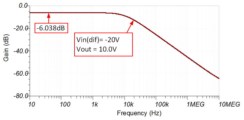
Transient ADC Input Settling Simulation Highest Sampling rate – 510ksps on ADS8568+OPA827
The following simulation shows settling to a 20V DC input signal with OPA827. This type of simulation shows that the sample and hold kickback circuit is properly selected to within ½ of a LSB (152µV). For detailed theory on this subject, refer to Introduction to SAR ADC Front-End Component Selection.
Transient ADC Input Settling Simulation Lower Sampling rate – 200ksps on ADS8568+OPA192
The following simulation shows settling to a 20V DC input signal with OPA192. This type of simulation shows that the sample and hold kickback circuit is properly selected to within ½ of a LSB (152µV).
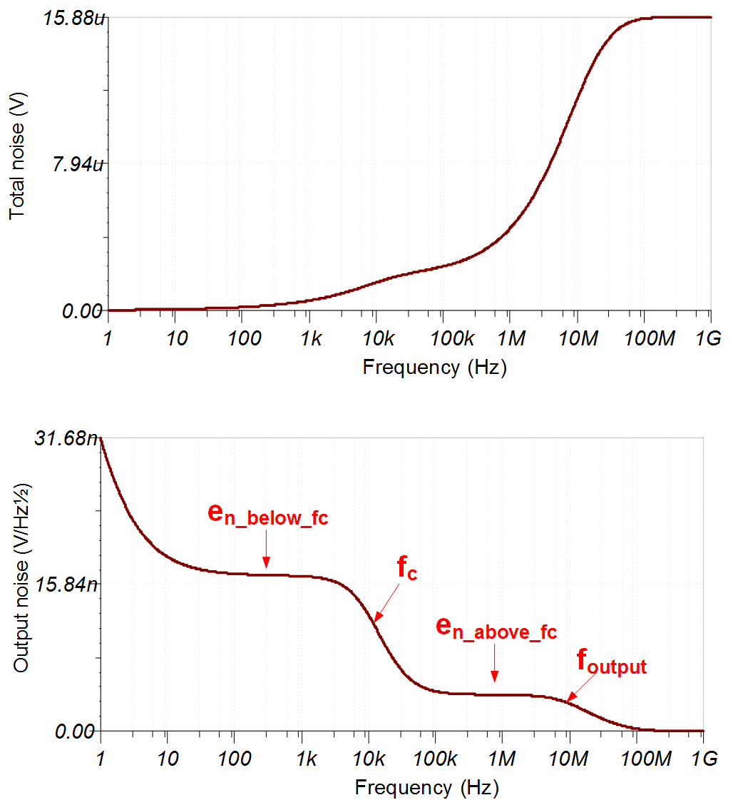
Noise Calculation
This section demonstrates a full-noise analysis including resistor noise. Also, look at the noise below fc (Noise Gain = 1.5), and the noise above fc (noise Gain = 1). In this example, the noise is dominated by wide band amplifier noise so the resistors do not contribute significantly. However, in many cases the resistor noise can be important, so the full noise calculation is provided. For more detailed theory on this subject, refer to Calculating the Total Noise for ADC Systems and Op Amps: Noise 1.
Bandwidth for feedback loop:
Noise from OPA827: 3.8nV/rtHz
Thermal noise density from feedback loop (Rf1 and Rg1 ) and RC non-inverting input (Rf2 and Rg2 ):
Noise from resistors on the non-inverting input is the same as noise from the feedback resistors.
Total noise (in gain) referred to output of amplifier:
Noise above fc is limited by the output filter (cutoff given below):
Total noise applied to input of the ADC:
Noise Simulation
The simulated results compare well with the calculated results (that is, simulated = 15.88µVrms, calculated = 14.128µVrms).
Stability Test
The phase margin for this OPA827 driving circuit is 67.1°, which meets the >45° requirement and is stable. For detailed theory explaining stability analysis, refer to Op Amps: Stability 1.
Design Featured Devices
| Device | Key Features | Link | Similar Devices |
|---|---|---|---|
| ADS8568(1) | 16-bit, 8 Channel Simultaneous-Sampling, Bipolar-Input SAR ADC | www.ti.com/product/ADS8568 | www.ti.com/adcs |
| OPA827 | Low-Noise, High-Precision, JFET-Input Operational Amplifier | www.ti.com/product/OPA827 | www.ti.com/opamp |
| OPA192 | High-Voltage, Rail-to-Rail Input/Output, 5µV, 0.2µV/°C, Precision operational amplifier | www.ti.com/product/OPA192 | www.ti.com/opamp |
Design References
For TI's comprehensive circuit library, refer to Analog Engineer's Circuit Cookbooks.
Link to Key Files (TINA)
Design files for this circuit – http://www.ti.com/lit/zip/sbac180.