Circuit for Driving a Switched-Capacitor SAR ADC With a Buffered Instrumentation Amplifier
| Input | ADC Input | Digital Output ADS8860 |
|---|---|---|
| –10mV | Out = 0.2V | 0A3DH or 262110 |
| 5mV | Out = 4.8V | F5C3H or 6291510 |
| AVDD | DVDD | Vref_INA | Vref | Vcc | Vee |
|---|---|---|---|---|---|
| 5.0V | 3V | 3.277V | 5.0V | 15V | –15V |
Design Description
Instrumentation amplifiers are a common way of translating low-level sensor outputs to high-level signals to drive an ADC. Typically, instrumentation amplifiers are optimized for low noise, low offset, and low drift. Unfortunately, the bandwidth of many instrumentation amplifiers may not be sufficient to achieve good settling to ADC charge kickback at maximum sampling rates. This document shows how a wide-bandwidth buffer can be used with an instrumentation amplifier to achieve good settling at high sampling rates. Furthermore, many instrumentation amplifiers are optimized for high voltage supplies and it can be required to interface the high voltage output (that is, ±15V) to a lower voltage amplifier (for example, 5V). This design shows how a current-limiting resistor can protect the amplifier from electrical overstress in cases where the instrumentation amplifier is outside the input range of the op amp. A related cookbook circuit shows a simplified approach that does not include the wide-bandwidth buffer (Driving a Switched-Capacitor SAR With an Instrumentation Amplifier circuit design). The simplified approach has limited sampling rate as compared to the buffered design. Note that the following circuit shows a bridge sensor, but this method could be used for a wide range of different sensors.
This circuit implementation is applicable in applications such as analog input modules, electrocardiograms (ECGs), pulse oximeters, lab instrumentation, and control units for rail transport.

| Specification | Calculated | Simulated |
|---|---|---|
| Sampling rate | 1Msps | 1Msps, settling to –44µV |
| Offset (ADC Input) | 40μV × 306.7 = 12.27mV | 16mV |
| Offset Drift | (0.4μV/°C) × 306.7 = 123μV/°C | N/A |
| Noise | 978μV | 586μVRMS |
Design Notes
- The bandwidth of instrumentation amplifiers is typically too low to drive SAR data converters at high data rates (the INA826 bandwidth is 10.4kHz for a gain of 305V/V in this example). Wide bandwidth is needed because the SAR has a switched capacitor input that needs to be charged during each conversion cycle. The OPA320 buffer was added to allow the ADC to run at full data rate (ADS8860 1Msps).
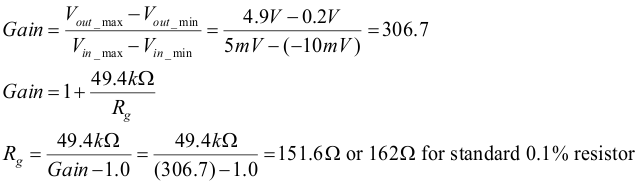
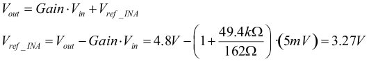
- Select the gain to achieve an input swing that matches the input range of the ADC. Use the instrumentation amplifier reference pin to shift the signal offset to match the input range. This is covered in the component selection section.
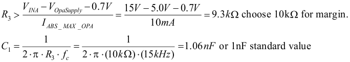
- The INA826 gain is scaled so that the op amp input voltage levels are inside the normal operating range of the amplifier. However, during power up or when a sensor is disconnected the output can drive to either power supply rail (±15V). The resistor R3 is used to limit the current . This is covered in the Overvoltage Protection Filter Between Instrumentation Amplifier and Op Amp section of this document.
- The buffer amplifier following the voltage divider is required for driving the reference input of most instrumentation amplifiers. Choose precision resistors and a precision low offset amplifier as the buffer. Refer to Selecting the right op amp for more details on this subject.
- Check the common mode range of the amplifier using the Common-Mode Input Range Calculator for Instrumentation Amplifiers software tool.
- Select COG capacitors for C1, and Cfilt to minimize distortion.
- Use 0.1% 20ppm/°C film resistors or better for the gain set resistor Rg. The error and drift of this resistor directly translates into gain error and gain drift.
- The Precision labs series: Analog-to-digital converters (ADCs) training video series methods for selecting the charge bucket circuit Rfilt and Cfilt. Refer to the Introduction to SAR ADC Front-End Component Selection for details on this subject.
Component Selection
- Find the gain set resistor for the
instrumentation amplifier to set the output swing to 0.2V to
4.8V.
- Find the INA826 reference voltage
(Vref) to shift the output swing to the proper voltage level.
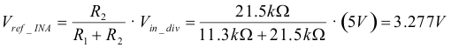
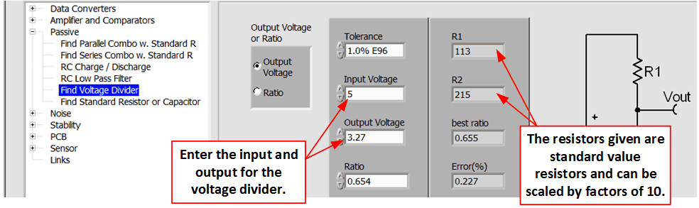
- Select standard value resistors to
set the INA826 reference voltage (Vref_INA = 3.27V). Use the Analog Engineer's Calculator ("Passive\Find
Voltage Divider" section) to find standard values for the voltage divider.
- Use the Common-Mode
Input Range Calculator for Instrumentation Amplifiers to
determine if the INA826 is violating the common mode range.

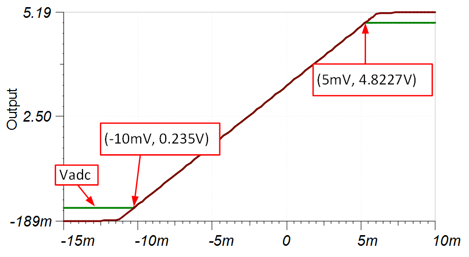
DC Transfer Characteristics
The following graph shows a linear output response for inputs from –5mV to +15mV. Refer to Determining a SAR ADC’s Linear Range when using Instrumentation Amplifiers for detailed theory on this subject. In cases where the INA826 output exceeds the op amp input range, the ESD diodes turn on and limit the input. The resistor R3 protects the amplifier from damage by limiting the input current (see the Overvoltage Protection Filter Between Instrumentation Amplifier and Op Amp section). The op amp output is inside the absolute maximum rating of the ADS8860 (–0.3V < VIN < REF +0.3V).
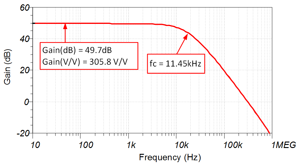
AC Transfer Characteristics
The bandwidth is simulated to be 11.45 kHz in this configuration. In this bandwidth it is not possible to drive the SAR converter at full speed. See the TI Precision Labs video series Op Amps: Bandwidth 1 for more details on this subject.
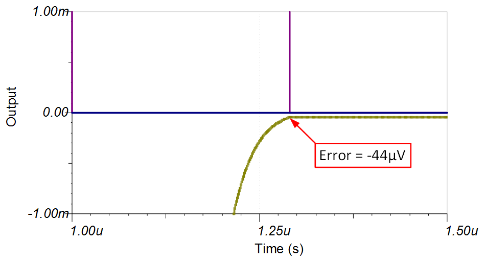
Transient ADC Input Settling Simulation
The OPA320 buffer (20MHz) is used because it is capable of responding to the rapid transients from the ADC8860 charge kickback. This type of simulation shows that the sample and hold kickback circuit is properly selected. Refer to Introduction to SAR ADC Front-End Component Selection for detailed theory on this subject.
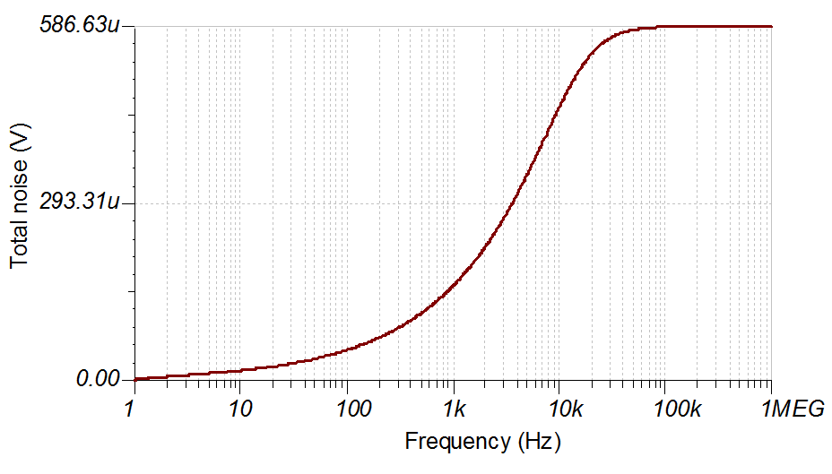
Noise Simulation
Use a simplified noise calculation for a rough estimate. We neglect the noise from the OPA192 as the instrumentation amplifier is in high gain so its noise is dominant.

Note that the calculated and simulated match well. Refer to TI Precision Labs - Op Amps: Noise 4 for detailed theory on amplifier noise calculations, and Calculating the Total Noise for ADC Systems for data converter noise.
Overvoltage Protection Filter Between Instrumentation Amplifier and Op Amp
The filter between the INA826 and OPA320 serves two purposes. It protects the OPA320 from overvoltage, and acts as a noise or anti-aliasing filter. Scale the INA826 gain so that under normal circumstances, the output is inside the range of the OPA320 (that is, 0V to 5V). Thus, normally the overvoltage signals applied to the input of the OPA320 is not seen. However, during power up or in cases where the sensor is disconnected, the INA826 output can be at either power supply rail (that is, ±15V). In overvoltage cases, the resistor (R3) limits current into the OPA320 for protection. The internal ESD diodes on the OPA320 turns on during overvoltage events and direct the overvoltage signal to the positive or negative supply. In the following example, the overvoltage signal is directed to the positive supply and the transient voltage suppressor (D1, SMAJ5.0A) turns on to sink the current. Note that the resistor is scaled to limit the current to the OPA320 absolute maximum input current (10mA). See TI Precision Labs - Op Amps: Electrical Overstress (EOS) for detailed theory on this subject.

Optional Input Filter
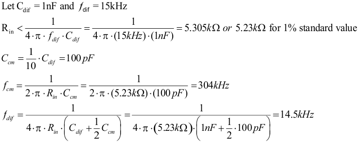
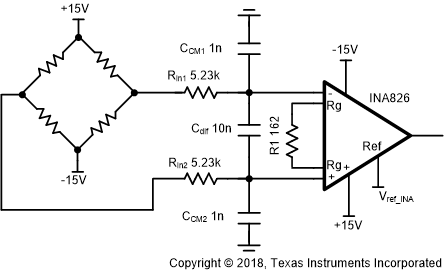
The following figure shows a commonly used instrumentation amplifier input filter. The differential noise is filtered with Cdif, and the common mode noise is filtered with Ccm1 and Ccm2. Note that it is recommended that Cdif ≥ 10Ccm. This prevents conversion of common mode noise to differential noise due to component tolerances. The following filter was designed for a differential cutoff frequency of 15kHz.
Design Featured Devices
| Device | Key Features | Link | Similar Devices |
|---|---|---|---|
| ADS8860 | 16-bit resolution, SPI, 1-Msps sample rate, single-ended input, Vref input range 2.5V to 5.0V. | 16-bit, 1MSPS, 1-channel SAR ADC with single-ended input, SPI and daisy chain | Precision ADCs |
| OPA192 | 8-kHz bandwidth, Rail-to-Rail output, 450-nA supply current, unity gain stable | High-Voltage, Rail-to-Rail Input/Output, 5µV, 0.2µV/˚C, Precision Operational Amplifier | Precision op amps (Vos<1mV) |
| INA826 | Bandwidth 1MHz (G=1), low noise 18nV/rtHz, low offset ±40µV, low offset drift ±0.4µV/°C, low gain drift 0.1ppm/°C. (typical values) | Precision, 200-μA Supply Current, 36-V Supply Instrumentation Amplifier | Instrumentation amplifiers |
Link to Key Files
Texas Instruments, source files for SBAC184, software support
Trademarks
All trademarks are the property of their respective owners.
Revision History
Changes from Revision A (March 2019) to Revision B (September 2024)
- Updated the format for tables, figures, and cross-references throughout the document Go
Changes from Revision * (February 2018) to Revision A (March 2019)
- Downstyle the title and changed title role to Data Converters. Added link to circuit cookbook landing page.Go
IMPORTANT NOTICE AND DISCLAIMER
TI PROVIDES TECHNICAL AND RELIABILITY DATA (INCLUDING DATASHEETS), DESIGN RESOURCES (INCLUDING REFERENCE DESIGNS), APPLICATION OR OTHER DESIGN ADVICE, WEB TOOLS, SAFETY INFORMATION, AND OTHER RESOURCES “AS IS” AND WITH ALL FAULTS, AND DISCLAIMS ALL WARRANTIES, EXPRESS AND IMPLIED, INCLUDING WITHOUT LIMITATION ANY IMPLIED WARRANTIES OF MERCHANTABILITY, FITNESS FOR A PARTICULAR PURPOSE OR NON-INFRINGEMENT OF THIRD PARTY INTELLECTUAL PROPERTY RIGHTS.
These resources are intended for skilled developers designing with TI products. You are solely responsible for (1) selecting the appropriate TI products for your application, (2) designing, validating and testing your application, and (3) ensuring your application meets applicable standards, and any other safety, security, or other requirements. These resources are subject to change without notice. TI grants you permission to use these resources only for development of an application that uses the TI products described in the resource. Other reproduction and display of these resources is prohibited. No license is granted to any other TI intellectual property right or to any third party intellectual property right. TI disclaims responsibility for, and you will fully indemnify TI and its representatives against, any claims, damages, costs, losses, and liabilities arising out of your use of these resources.
TI’s products are provided subject to TI’s Terms of Sale (www.ti.com/legal/termsofsale.html) or other applicable terms available either on ti.com or provided in conjunction with such TI products. TI’s provision of these resources does not expand or otherwise alter TI’s applicable warranties or warranty disclaimers for TI products.
Mailing Address: Texas Instruments, Post Office Box 655303, Dallas, Texas 75265
Copyright © 2024, Texas Instruments Incorporated