Active-Filtering Circuit for Audio DACs
Design Goals
| Filter Input | Cutoff Frequency | Filter Gain |
|---|---|---|
| 4VPP, 1.42VRMS | –3dB at 23kHz | –1V/V, 0dB |
Design Description
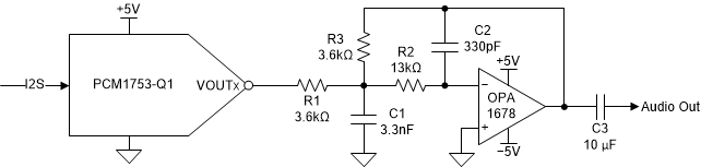
This circuit shows the implementation of a second-order active-filter for audio digital-to-analog converter (DAC) applications. In applications such as automotive head units, home theater soundbars, and AV receivers, it is critical to minimum undesirable noise in the audible range, approximately 20Hz to 22kHz. For this reason, many delta-sigma type audio DACs implement noise shaping techniques that force the noise generated by the over-sampling functionality of the DAC outputs side of the audible range, this is process is called 'noise-shaping,' while the actual noise is called 'out-of-band noise.' Many common audio DACs, such as the PCM1753-Q1, have noise-shaping that forces the out-of-band noise to approximately 50% the sampling rate, fS, of the digital source. While this noise is not generally considered audible, it can have detrimental effects on the amplifier circuits that are found on the output of audio DACs. For example, this out-of-band noise may be aliased by class-D amplifiers that operate at higher frequencies back into the audible range. In addition, this noise would also experience the same analog gain of the output amplifiers if no filtering is implemented. The second-order active-filter design allows a higher level of noise attenuation closer to the audible band than a simple, first-order RC filter. In addition, it allows the audio output of the system to have a lower impedance and current drive than the audio DAC can provide due to the output drive capabilities of the op amp featured in the filter.
Design Notes
- It is important to note that the fC of the design is optimized for a sample rate of at least 44.1kHz, which is common in audio systems. The fC should be approximate 50% of the sample rate, to attenuate the out-of-band noise from the delta-sigma modulator. If a higher frequency sample rate is used, move the cutoff frequency further out in the frequency domain to allow a wider bandwidth from the audio DAC.
- Not all audio DACs require a second-order active filter. Some audio DACs feature different noise-shaping architectures that moves the out-of-band noise further away from the audible range, meaning that a simple RC filter may be enough to attenuate the unwanted noise.
- Most audio system feature a DC blocking capacitor to allow the audio output to be ground centered. In this design, put the blocking capacitor directly on the output of the DAC, but as the amplifier will also have some small offset, the capacitor is generally placed directly on the output of the filter or the input of the amplifier or headphone driver that would proceed the active filter.
Design Steps
- Select a DAC based on the needs of the application. Consider the required signal-to-noise ratio (SNR), total harmonic distortion and noise (THD+N), and supported I2S interface sample rates. While most audio DACs support rates ranging from 16kHz to 192kHz, not all support rates like 384kHz or 768kHz. Higher rates result in noise shaping that moves the out-of-band noise further from the audible range, but not all audio sources can provide them.
- The amplifier selected for the design (OPA1678) is a CMOS input amplifier. CMOS input amplifiers have lower current noise at the inputs of the amplifier at lower frequencies than JFET type amplifiers. The current-noise translates to voltage-noise on the output as the filter features input large resistance values, so it is important to select an amplifier with low current-noise.
- Select the resistor and capacitor
values for the filter to have a –3dB point at approximately 23kHz. The
fC of the circuit can be calculated using the following equation:
- The capacitors used for the filter must be COG/NP0 type ceramics. COG/NP0 type capacitors have a lower voltage coefficient of capacitance, meaning that the capacitive value of the component is less impacted by the voltage bias across the device. As the capacitors are key for performance of the filter, other types of ceramic capacitors should be avoided in the signal path.
- Thin-film resistors are recommended for the resistive elements
in the filter. All resistors feature voltage noise, which is well understood to
be dependent on resistance and temperature, as shown in the first equation
following. But resistors also have a current noise, which is dependent on the
voltage across the resistor, frequency, and a constant, C, that is
dependent on the material of which the resistor is composed, as shown in the
second equation that follows. ST = 4kRT
where
- k is Boltzmann's constant
- R is resistance
- T is temperature
SE = ( C × U2 ) ÷ ƒwhere
- C is a constant derived from the resistor material
- U is the differential voltage across the resistor
- ƒ is the frequency
Simulated Filter Response
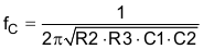
The following graph shows the simulated filter response of the second-order active filter as well as the response of a simple, first order RC filter with approximately the same fC. Note that the filter roll-off for the first order filter is –20dB/decade, while the roll-off for the active filter is –40dB/decade.
Simulated Noise Performance
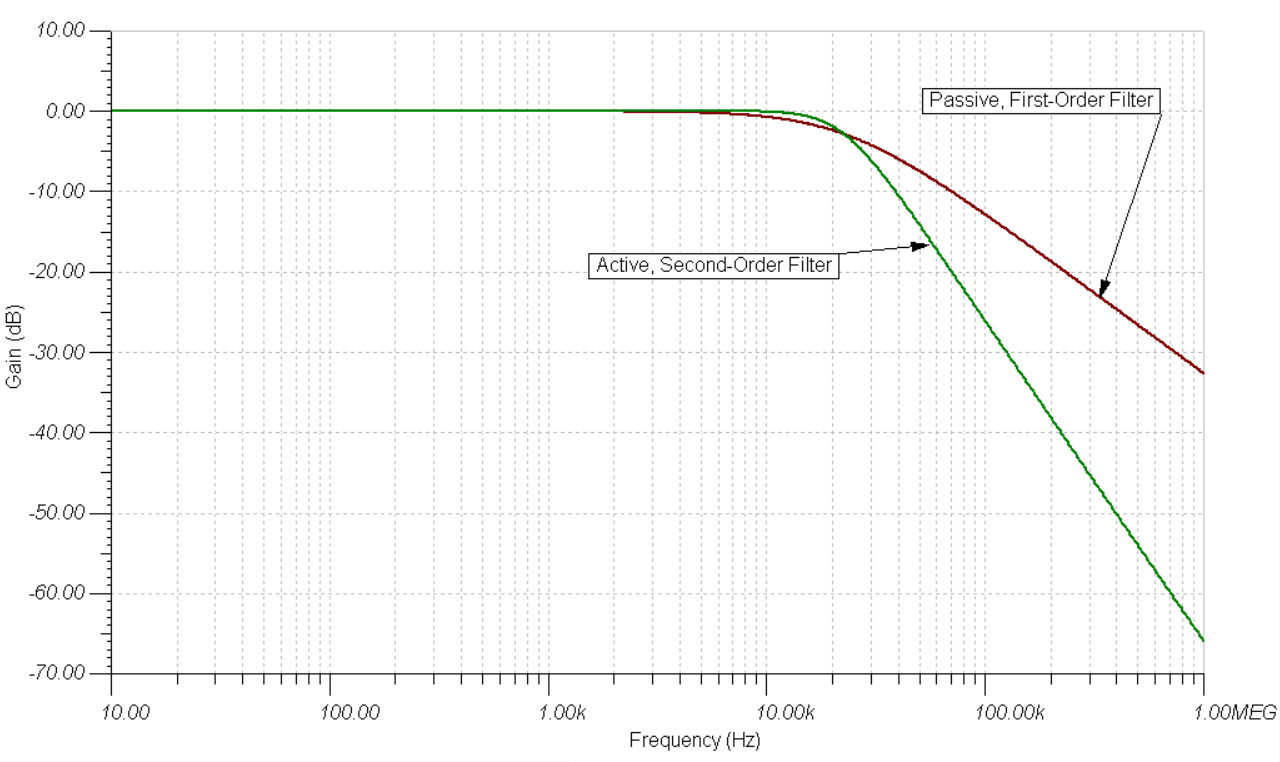
The following graph shows the simulated total noise contribution of the circuit, with the exception of the DAC. The was simulated using the OPA1678, which is specified as having 4.5nV/√ Hz at 1kHz, and the OPA1612, which is specified as having 1.1nV/√ Hz at 1kHz. The results show that the contribution of the current noise in the system result in a greater total noise in the OPA1612 versus the OPA1678, even though the OPA1612 has lower voltage noise.
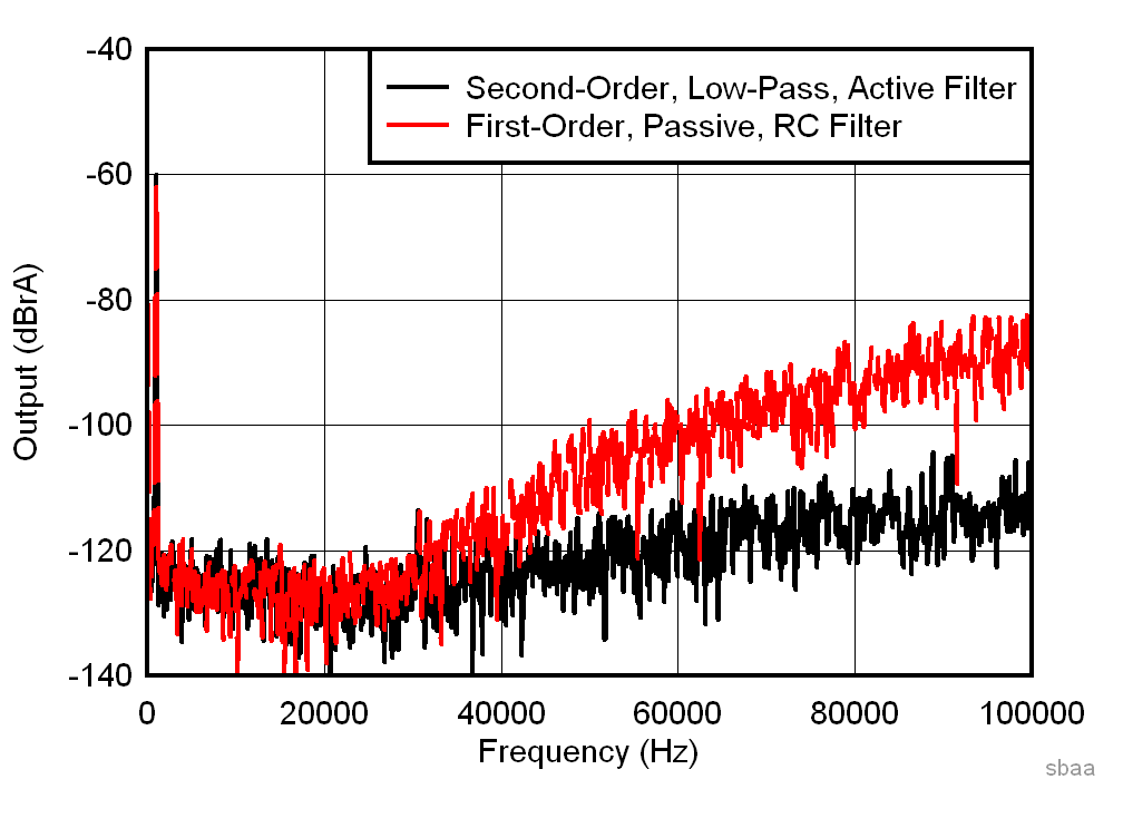
Measured Output Spectrum
The output of the DAC was measured in the frequency domain with the second-order, active-filter as well as the first-order RC filter. The output of the DAC was set to –60dB full-scale amplitude at 1kHz frequency with a sample rate of 48kHz.
The graph shows that the out-of-band noise begins to increase at around 24kHz, which is expected given the noise-shaping of the PCM1753-Q1. The second-order filter has approximately a 20dB lower output at 100kHz when compared to the RC filter.
Design Featured Devices
| Device | Key Features | Link | Other Possible Devices |
|---|---|---|---|
| PCM1753-Q1, PCM1754-Q1 (1) |
24-bit resolution, 106dB typical SNR, 0.002% typical THD+N, single-ended, voltage-output, audio DAC | Automotive 106-dB SNR stereo digital-to-analog converter (DAC) (software control) | Audio DACs |
| OPA1678 | Low distortion, low noise, low input current, dual amplifier for audio applications | Single Channel 450nA Precision Nanopower Operational Amplifier | Audio Op-Amps Overview |
Design References
Texas Instruments, SBAM410 circuit source files, software
Other Links:
Texas Instruments, Precision DAC Learning Center, portfolio overview
Texas Instruments, Designing a Premium Audio System, video
Texas Instruments, Audio DACs, portfolio overview
Trademarks
All trademarks are the property of their respective owners.
