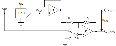
Circuit for Differential Output From a Single-Ended Precision DAC
| Power Supply | DAC Output | Offset Range |
|---|---|---|
| VCC: 10V, VSS: –10V, VDD: 5V | 0V to 5V | ±5V |
Design Description
This single-ended to differential conversion circuit features two operational amplifiers (op amp). It generates a bipolar differential output from a unipolar digital-to-analog converter (DAC) channel. These types of circuits are very useful in low-noise applications like Optical module, Metro data center interconnect, Ultrasound scanners, and X-ray systems. While another design approach using a fully-differential amplifier (FDA) is good for AC performance, the op amp approach will achieve best DC characteristics. Nevertheless, the specific op amp or FDA will impact the comparison of the two topologies.
Design Notes
- Choose a DAC with required resolution and output range
- Select an op amp to meet the
system specifications considering the following key requirements:
- Swing to rail: For 5-V supply rails it is common to use a rail-to-rail zero-crossover distortion device (for example, OPA320 and OPA365)
- Offset voltage and drift: One of the advantages of this circuit over the FDA approach is that some op amps can have very good DC performance
- Bandwidth and quiescent current: Another advantage of this circuit over the FDA approach is that a wide range of op-amp bandwidth and related quiescent currents are available. For lower sampling rate, a low-bandwidth, low-current op amp may be an optimal choice
- Choose R1 and R2 to minimize thermal noise at the output
Design Steps
- Select a DAC such as DAC80501 that is a 16-bit single channel buffered voltage output DAC with a 2.5-V internal reference. The reference output can also be used as the common-mode voltage (VCM)
- Select a low-distortion op amp such as OPA320
- The DC transfer function of the circuit is described with the
following equations:

- R1 and R2 is chosen as 1kΩ to have a gain of 1 and to minimize noise. Use 0.1% tolerance to minimize gain error.
- The thermal noise contributed by U1 to the
differential output has two paths: directly through U1 and with
inversion through U2. Both these noise are correlated and hence they
will add directly. DAC80501 has an output noise density
(en-DAC) of 74nV/√ Hz and OPA320
has a noise density (en-AMP) of 7nV/√
Hz. The noise gain of U1 (Gn-U1)
is 1. So, the total noise density contributed by output of U1
(en-U1) is given by:

- The thermal noise contributed by the gain resistors
R1 and R2, (en-R) is given by:

- The uncorrelated noise density contributed by U2
(en-U2) is a combination of the thermal noise of the
gain resistors (en-R), thermal noise of U2
(en-AMP), and the noise contributed by VCM
when fed through the VREF output of DAC80501
(en-VREF). en-VREF is 140nV/√
Hz. The noise gain of U2
(Gn-U2), that is, 1+(R2/R1) is 2.
So, en-U2 is written as:

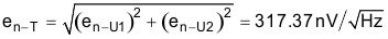
- Finally, combining the noise from U1 and U2, we get
the total noise density at the differential output
(en-T):
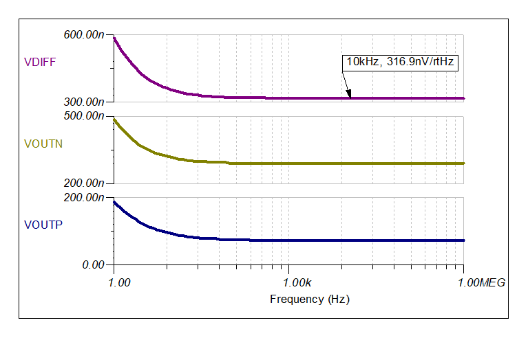
The simulated value for the thermal noise at the differential output is shown in the following figure. The simulated value 316.9nV/√ Hz is close to the calculated value. The thermal noise for the DAC output and VREF output were emulated with equivalent resistors for noise simulation.
Thermal Noise Density at The Differential Output (VCM = VREF)
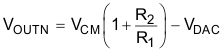
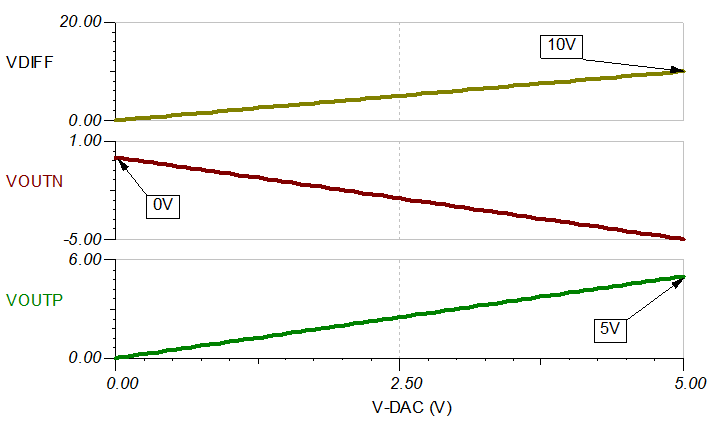
DC Transfer Characteristics (VCM = 0V)
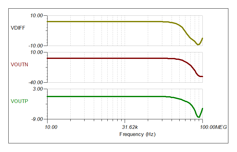
Frequency Response (Amplitude)
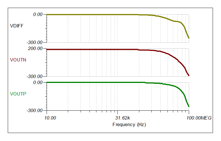
Frequency Response (Phase)
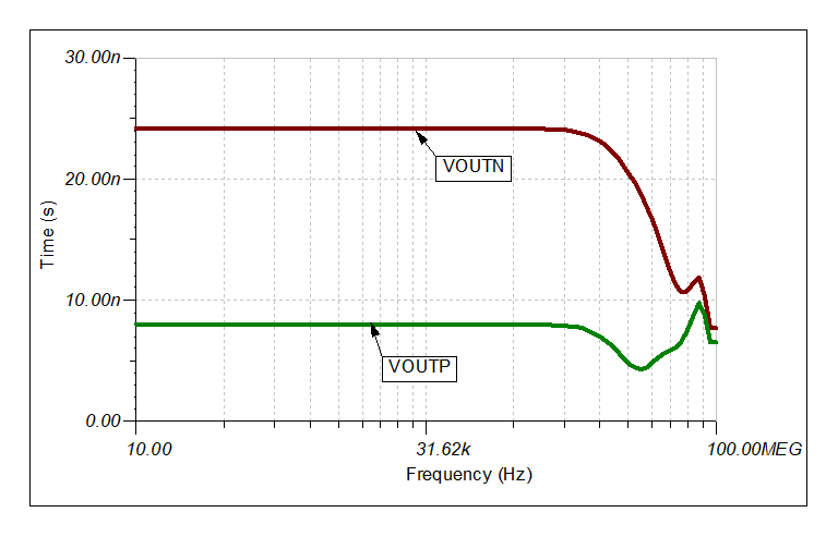
Group Delay
Group delay is the time delay between the applied input signal and the output signal. All amplifiers and filters have a group delay. Group delay is highlighted for this circuit because the inverting and noninverting path both have different group delays. This can create distortion for higher frequency signals. See the group delay in time domain plot for additional detail.
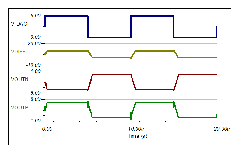
Output Transient Response
Design Featured Devices and Alternative Parts
| Device | Key Features | Link |
|---|---|---|
| DAC80501 | 16-bit, 1-LSB INL, digital-to-analog converter (DAC) with precision internal reference | True 16-bit, 1-ch, SPI/I2C, voltage-output DAC in WSON package with precision internal reference |
| DAC80508 | 8-channel, true 16-bit, SPI, voltage-output DAC with precision internal reference | 16-Bit, Ultralow Glitch, Voltage Output, Digital to Analog Converter |
| DAC8562 | 16-bit, dual-channel, low-power, ultra-low glitch, voltage output DAC with 2.5V, 4ppm/°C reference | 16-bit, dual-channel, low-power, ultra-low glitch, voltage output DAC with 2.5V, 4ppm/°C reference |
| OPA320 | Precision, zero-crossover, 20MHz, 0.9pA Ib, RRIO, CMOS operational amplifier | Precision, zero-crossover, 20MHz, 0.9pA Ib, RRIO, CMOS operational amplifier |
| OPA365 | 2.2V, 50MHz, low-noise, single-supply rail-to-rail operational amplifier | 2.2V, 50MHz, Low-Noise, Single-Supply Rail-to-Rail Operational Amplifier |
Link to Key Files
Texas Instruments, TINA SBAM419, source files
