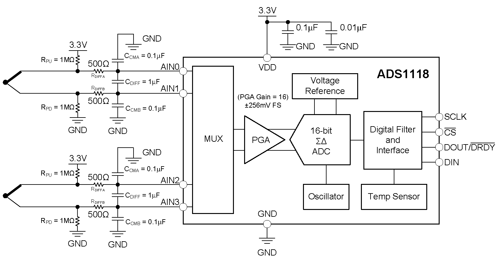
Two-channel, K-type thermocouple measurement circuit with internal temperature sensor CJC
| Input Measurement | ADC Input Voltage | ADC Digital Output |
|---|---|---|
| T = –270°C | AINP – AINN = –6.5mV | FCC0H or –83210 |
| T = 1370°C | AINP – AINN = 55mV | 1B80H or 704010 |
| VDD | GND | |
|---|---|---|
| 3.3V | 0V | |
Design Description
This cookbook design describes a temperature measurement circuit with two thermocouples using the ADS1118. Thermocouple voltage measurements are made with the ADS1118 internal voltage reference, while cold-junction compensation (CJC) measurements are made with the onboard temperature sensor. Two channels of the ADC are used for two K-type thermocouples with a temperature measurement range from –270°C to 1370°C. Included in this design are ADC register settings to configure the device and pseudo code is provided to configure and read from the device. This circuit can be used in applications such as analog input modules for PLCs, lab and field instrumentation, and factory automation and control. For more information about using precision ADCs with thermocouples, see A Basic Guide to Thermocouple Measurements.
Design Notes
- Use supply decoupling capacitors for the supply. VDD must be decoupled with at least a 0.1-μF capacitor to GND. See ADS1118 Ultrasmall, Low-Power, SPI™-Compatible, 16-Bit Analog-to-Digital Converter with Internal Reference and Temperature Sensor for details on power supply recommendations.
- When possible, use C0G (NPO) ceramic capacitors for input filtering. The dielectric used in these capacitors provides the most stable electrical properties over voltage, frequency, and temperature changes. Because of size, this may not always be practical and X7R capacitors are the next best alternative.
- Cold-junction compensation is required for accurate measurement of the thermocouple temperature.
- The K-type thermocouple is chosen as it has a large input range and thermocouple voltage. Other thermocouples have different sensitivities and error tolerances. For measurements with other thermocouples and a guide to use them, see A Basic Guide to Thermocouple Measurements.
- Conversion tables and polynomial equations used to determine thermocouple temperature from the thermoelectric voltage is found at the NIST website. Additionally, use the Analog Engineer's Calculator to determine some thermocouple conversions.
Component Selection
- Identify the range of operation for the thermocouple.
The K-type thermocouple has a range of approximately −6.5mV to +55mV if the temperature measurement range is from −270°C to 1370°C. This range is used to maximize the resolution of the measurement, considering the full-scale range of the ADC.
- Determine gain and input range of the ADC.
In the ADS1118, the programmable gain amplifier (PGA) is implemented through scaled capacitive sampling, not as a true amplifier. With this PGA, the input range extends to the full supply range, but has less amplification and lower input impedance. In this device, the maximum amplification gives a full scale range of ±0.256V. This is much larger than the range of −6.5mV to +55mV for the thermocouple. While it is not possible to over-range the PGA, the measurement uses a limited portion of the full scale range. Comparing the thermocouple range to the full-range, the percent of the usable ADC range can be calculated:
% of usable ADC range = [55mV–(–6.5mV)]/[0.256mV–(–0.256mV)] • 100% = 12.0%Number of ADC codes in measurement range = 0.12 × 216 = 7864With a range of −270°C to 1370°C for the thermocouple, 7864 codes are used to represent a temperature range of 1640°C. This equates to approximately 0.21°C per ADC code which is enough for most thermocouple applications.
In other precision ADCs, the PGA is implemented similar to an instrumentation amplifier. If using a different ADC, calculate the maximum gain allowed without over-ranging the PGA based on the maximum thermocouple output voltage. Then, verify that the thermocouple biasing is near mid-supply so that the input signal is in the common-mode input range of the PGA.
- Set up the resistor biasing to establish the input DC level and
burnout detection.
Equal biasing resistors are tied from either end of the thermocouple and to GND and VDD. In normal operation, the resistors set the DC biasing point of the thermocouple to near mid-supply. If the thermocouple burns out and becomes an open circuit, the resistors pull apart the thermocouple leads to either supply. These resistors are set high (often 500kΩ to 10MΩ) to reduce the bias current going through the thermocouple. Resistor bias current reacting with the thermocouple lead resistance cause measurement error. However, the resistors must also be low enough to provide sufficient bias current to overcome any input current from the resistor.
In this design, biasing resistors are chosen to be 1MΩ. This value sets the resistor biasing current to a low 1.65µA. However, in the case of a burned out thermocouple, 1MΩ provides enough current to separate the ADC inputs against the 710kΩ equivalent input impedance of the ADS1118.
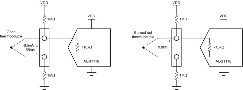
In the case of the good thermocouple, the thermocouple voltage has a range of –6.5mV to 55mV. The remaining 3.3V of the VDD supply is dropped equally between the biasing resistors. With 1-MΩ bias resistors, the thermocouple voltage has a DC operating point near mid-supply at 1.65V.
In the case of a burned out thermocouple, the open circuit creates a voltage divider with the two 1MΩ around the 710-kΩ equivalent input impedance. The ADC input voltage with a burned out thermocouple may be calculated as:
ADC input voltage = 3.3V × [710kΩ ÷ (1MΩ + 710kΩ + 1MΩ)] = 0.85VIf the thermocouple burns out, the ADC input voltage is 0.86V, which is much larger that the positive full-scale reading of the ADC. The ADC reports a reading of 7FFFh to indicate a burnout condition.
- Select values for the differential and common-mode filtering
for the ADC inputs and reference inputs.
If there is input filtering, the input current reacts with any series filter resistance to create an error. For the ADS1118, the input current is modeled as an equivalent differential input impedance. As previously mentioned, the equivalent differential input impedance is typically 710kΩ. For this reason, the input series resistance is kept low or the added voltage appears as a gain error.
This design includes differential and common-mode input RC filtering. The bandwidth of the differential input filtering is set to be at least 10 × higher than the data rate of the ADC. The common-mode capacitors are selected to be 1/10 of the value the differential capacitor. Because of capacitor selection, the bandwidth of common-mode input filtering is approximately 20 × higher than the differential input filtering.
With input filtering, differential signals are attenuated at a lower frequency than the common-mode signals, which are significantly rejected by the PGA of the device. Mismatches in common-mode capacitors cause an asymmetric noise attenuation, appearing as a differential input noise. With a lower bandwidth for differential signals, the effects from the mismatch of input common-mode capacitors are reduced. Input filtering for the ADC inputs and reference inputs are designed for the same bandwidth.
In this design, the data rate is chosen to be 8SPS. For the ADC input filtering, the bandwidth frequency for the differential and common-mode filtering is approximated in the following equations:
fIN_DIFF = 1 ÷ [2 × π × CDIFF × (2 × RDIFF)]fIN_CM = 1 ÷ (2 × π × CCM × RDIFF)For the ADC input filtering, RIN = 500Ω, CIN_DIFF = 1µF, and CIN_CM = 0.1µF. This sets the differential filter bandwidth to 160Hz and the common-mode filter bandwidth to 3.2kHz.
- Use cold-junction compensation to calculate the actual
thermocouple voltage based on the cold-junction temperature.
To get a precise measurement from a thermocouple, cold-junction compensation must be performed to get an accurate temperature measurement. An accurate measurement of the cold-junction where the thermocouple leads are tied is required. You cannot simply add the temperature of the cold-junction to the temperature computed from the thermocouple voltage. To accurately determine the thermocouple temperature, the proper method is to:
- Convert the cold-junction temperature (TCJ) to a voltage (VCJ)
- Add the cold-junction voltage to the measured thermocouple voltage (VCJ + VTC)
- Convert the summed cold-junction voltage and thermocouple voltage to the thermocouple temperature (TTC)
The following flow diagram shows the conversion method to determine the actual temperature of the thermocouple based on the ADC measurements.
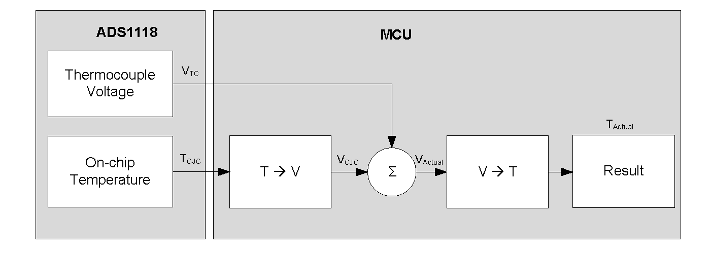
Conversion tables and polynomial equations used to determine thermocouple temperature from the thermoelectric voltage are found at the NIST website.
Because the ADS1118 has an accurate internal temperature sensor, use a measurement. The internal temperature sensor has a typical accuracy of 0.2°C for a range of 0°C to 70°C. This accuracy is preferred for the cold-junction measurement. However, the device requires a good thermal contact to the connection for the thermocouple cold-junction. Any error in the cold-junction measurement yields an error in the resulting temperature measurement.
For more information about thermocouples and the cold-junction compensation measurement, see A Basic Guide to Thermocouple Measurements.
Measurement Conversion
Conversions for the thermocouple voltage are relatively straight forward based on the full-scale range setting of the ADC. In this design, the smallest full-scale range is used (±0.256V).
Measurement 1 (Thermocouple 1):
Measurement 2 (Thermocouple 2):
Conversions for the internal temperature sensor require some data manipulation. Temperature data from the ADC are represented as a 14-bit result that is left-justified within the 16-bit conversion result. Data are output starting with the most significant byte (MSB). When reading the two data bytes, the first 14 bits are used to indicate the temperature measurement result. One 14-bit LSB equals 0.03125°C and negative numbers are represented in binary twos complement format.
Measurement 3 (Internal Temperature Sensor):
Output Code 3 is the first 14 bits of the two byte output data from the ADC. For more information about the ADS1118 and the internal temperature sensor see ADS1118 Ultrasmall, Low-Power, SPI™-Compatible, 16-Bit Analog-to-Digital Converter with Internal Reference and Temperature Sensor.
Register Settings
| Bit | Field | Setting | Description |
|---|---|---|---|
| 15 | SS | 1 | Start a single conversion |
| 14:12 | MUX[2:0] | 000 | AINP is AIN0 and AINN is AIN1 for thermocouple 1 |
| 11:9 | PGA[2:0] | 110 | FSR is ±0.256V |
| 8 | MODE | 1 | Power-down and single-shot mode |
| 7:5 | DR[2:0] | 000 | 8SPS |
| 4 | TS_MODE | 0 | ADC mode |
| 3 | PULL_UP_EN | 1 | Pullup resistor enabled on DOUT/ DRDY pin |
| 2:1 | NOP[1:0] | 01 | Valid data, update the Config register |
| 0 | Reserved | 1 | Always write 1h |
| Bit | Field | Setting | Description |
|---|---|---|---|
| 15 | SS | 1 | Start a single conversion |
| 14:12 | MUX[2:0] | 011 | AINP is AIN2 and AINN is AIN3 for thermocouple 2 |
| 11:9 | PGA[2:0] | 110 | FSR is ±0.256V |
| 8 | MODE | 1 | Power-down and single-shot mode |
| 7:5 | DR[2:0] | 000 | 8SPS |
| 4 | TS_MODE | 0 | ADC mode |
| 3 | PULL_UP_EN | 1 | Pullup resistor enabled on DOUT/ DRDY pin |
| 2:1 | NOP[1:0] | 01 | Valid data, update the Config register |
| 0 | Reserved | 1 | Always write 1h |
| Bit | Field | Setting | Description |
|---|---|---|---|
| 15 | SS | 1 | Start a single conversion |
| 14:12 | MUX[2:0] | 011 | AINP is AIN2 and AINN is AIN3 (ignored by TS_MODE) |
| 11:9 | PGA[2:0] | 110 | FSR is ±0.256V (ignored by TS_MODE) |
| 8 | MODE | 1 | Power-down and single-shot mode |
| 7:5 | DR[2:0] | 000 | 8SPS |
| 4 | TS_MODE | 1 | Temperature sensor mode (bypasses MUX[2:0]) |
| 3 | PULL_UP_EN | 1 | Pullup resistor enabled on DOUT/ DRDY pin |
| 2:1 | NOP[1:0] | 01 | Valid data, update the Config register |
| 0 | Reserved | 1 | Always write 1h |
Pseudo Code Example
The following shows a pseudo code sequence with the required steps to set up the device and the microcontroller that interfaces to the ADC to take subsequent readings from the ADS1118 in single-shot conversion mode.
Data read back and device configuration are done with 32-bit transmission cycle with Configure register read back. The ADS1118 is configured to measure the thermocouple voltages with a full-scale range of ±256mV and a data rate of 8SPS. The device cycles from reading the voltage of thermocouple 1, the voltage of thermocouple 2, and then the ADS1118 internal temperature sensor. After taking all three readings, cold-junction compensation is used to convert the thermocouple voltages to the thermocouple temperatures.
Configure microcontroller for SPI mode 1 (CPOL = 0, CPHA = 1)
Set CS low; // Start conversions
Send 8D0B8D0B;  //Start conversion for thermocouple 1
// Use 32-bit data transmission cycle with Config register readback
// The first iteration of the loop has no data readback
Set CS high;
Loop
{
Wait 69ms // Wait for typical data period +10% for internal oscillator variation
Set CS low;
Send BD0BBD0B; // Read data for thermocouple 1, start conversion for thermocouple 2,
Set CS high;
Wait 69ms;
Set CS low;
Send 8D1B8D1B; // Read data for thermocouple 2, start conversion for temperature sensor,
Set CS high;
Wait 69ms;
Set CS low;
Send 8D0B8D0B // Read data temperature sensor, Start conversion for thermocouple 1
Set CS high;
// Cold-junction compensation to determine thermocouple temperature
Convert thermocouple 1 ADC data to voltage;
Convert thermocouple 2 ADC data to voltage;
Convert temperature sensor data to temperature;
Convert temperature sensor data to thermoelectric voltage; // By lookup table or calculation
Add thermocouple 1 voltage to temperature thermoelectric voltage;
Convert resulting voltage for thermocouple 1 to temperature; // By lookup table or calculation
Add thermocouple 2 voltage to temperature thermoelectric voltage;
Convert resulting voltage for thermocouple 2 to temperature; // By lookup table or calculation
}
Design Featured Devices
| Device | Key Features | Link | Other Possible Devices |
|---|---|---|---|
| ADS1118 | Ultrasmall, low-power, SPI™-compatible, 16-bit analog-to-digital converter with internal reference and temperature sensor | 16-bit, 860-SPS, 4-channel, delta-sigma ADC with PGA, oscillator, VREF, temp sensor and SPI | Precision ADCs (1) |
Additional Resources
- Texas Instruments, ADS1118 Evaluation Module, product overview
- Texas Instruments, ADS1118EVM User Guide and Software Tutorial, user's guide
- Texas Instruments, A Basic Guide to Thermocouple Measurements, application note
- Texas Instruments, Analog Engineer's Calculator, tool overview
- Texas Instruments, Simple thermocouple measurement reference design, less than 1°C accuracy, product overview
Trademarks
All trademarks are the property of their respective owners.