Circuit for Protecting Low-Voltage SAR ADC From Electrical Overstress With Minimal Impact on Performance
| Single-Ended Input (VREF = +5V) |
ADC Input | Digital Output ADS8860 |
|---|---|---|
| VinMax = +5V | AINP = +5V, AINN = 0V | FFFFH |
| VinMin = 0V | AINP = 0V, AINN = 0V | 0000H |
| Vcc on OPA828 | Vee on OPA828 | Clamp Voltage and Reference | ADS8860 AVDD and DVDD |
|---|---|---|---|
| +12V | –12V | +5V | +3V |
Design Description
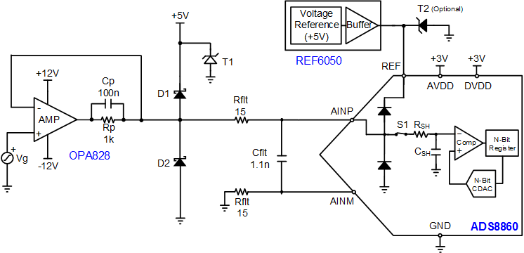
This cookbook circuit describes how to connect a high-voltage amplifier (for example, ±12V) to a low voltage ADC (for example, 0V to 5V) and clamp the output voltage of the amplifier to protect the ADC from electrical overstress damage. Furthermore, this document shows the impact that the protection clamp has on system performance. This circuit is useful in test and measurement, and factory automation and control.
This example circuit connects the OPA828 to the ADS8860. The OPA828 device has ±12-V supplies and the ADS8860 device has 0-V to 5-V input range. Normally, the amplifier supplies are matched to the ADC input range to prevent overstress of the inputs, but in some cases it may be useful to connect a higher voltage amplifier to a low-voltage ADC. Under a fault condition, when the output of the amplifier is above 5V or below ground, the diodes D1 and D2 turn on and limit the ADC input voltage to safe levels. The resistor Rp limits the output current under fault conditions. The Rp resistor is connected inside the amplifier feedback so that the impedance is reduced by the amplifiers feedback, under normal conditions. Keeping Rp in the feedback improves AC system performance (SNR and THD). This protection method is suitable for other precision SAR ADC with a switched capacitor input.
Specifications
| Specification | Goal | Calculated | Simulated | Measured |
|---|---|---|---|---|
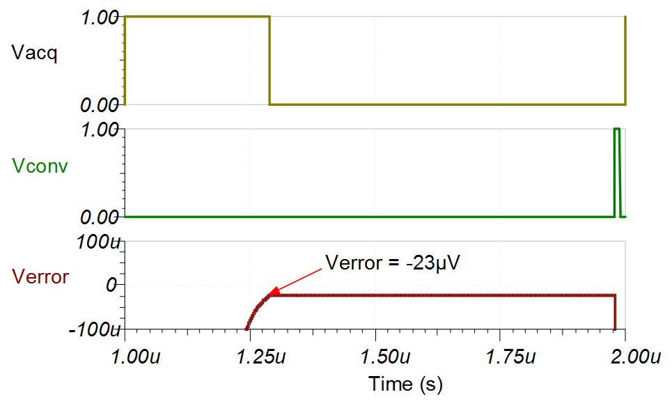
| Transient Settling Error | < 1/2LSB (< 38.15µV) | 0.3 LSB (23.1µV) | ||
| THD | < –108dB | –113.7dB | ||
| SNR | > 92dB | 93.3dB | ||
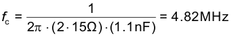
| Bandwidth | > 1MHz | 4.82MHz | 5.08MHz | |
| Noise | < 1/2LSB (< 38.15µV) | 11.3µVRMS | 10.04µVRMS |
Design Notes
- The BAT54 diode is selected for D1 and D2 because of its lower forward voltage, low leakage current, and low capacitance as the capacitance on the diode is nonlinear and can introduce distortion.
- The OPA828 device is a high bandwidth (45MHz) precision amplifier which is good enough to drive the 16-bit precision SAR ADC ADS8860 device. See the TI Precision Labs – ADCs training video: Introduction of Selecting and Verifying the Driver Amplifier for details.
- Select the C0G type capacitor for Cfilt to minimize the distortion.
Component Selection
- The following table lists the
maximum output voltage and current for the OPA828 amplifier. The table also
lists the absolute maximum specifications for the ADS8860 ADC. The ADC input
voltage range is set as the maximum voltage before turning on the internal ESD
diodes. The input current range is the maximum current the internal ESD diodes
can support continuously.
OPA828 Output ADS8860 Absolute Maximum Ratings OPA828 maximum output voltage: –12V ≤ Vo< 0V AINP or AINN –0.3V VADC_in_min (EOS voltage range - Vo ) +5V < Vo ≤ +12V to GND +5.3V VADC_in_max OPA828 maximum output current: –50mA Input current –10mA IADC_in_min (Short-circuit current - Isc ) +50mA +10mA IADC_in_max - Select a diode with a low forward drop, low leakage current, sufficient forward current, and low capacitance. Generally, a Schottky diode is used for its low forward drop. See the video series on EOS Protection for ADCs for details on selection of the diode and other information on overstress protection. In this example, the BAT54 Schottky diode is selected as it has a good forward voltage drop as well reasonable leakage current and capacitance. The BAT54 is a common choice for EOS protection.
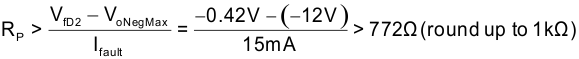
- For this circuit, a –12-V output
from the OPA828 amplifier is limited to –0.42V, and a 12-V output is limited to
5.42V. The largest voltage across Rp occurs when the amplifier output is at
–12V. Hence, Rp is determined by the following equation:
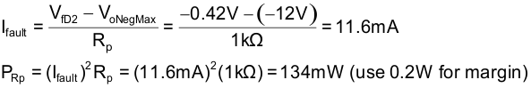
- In the following equation, the
fault current and power dissipated is calculated in Rp during an electrical
overstress fault event. The objective is to make sure that the correct power
rating is used on the resistor Rp.
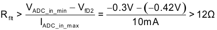
- The resistor Rfilt acts as a charge
bucket filter and also to limit the current under a fault condition. First, a
minimum value of Rfilt is determined for fault protection by assuming D2 has a
0.42-V drop on it and the internal ESD diode has 0.3V on it. Using this voltage
and the absolute maximum input current rating, the minimum value of Rfilt for
current limiting is selected (12Ω).
- Next, a TINA-TI SPICE-based analog simulation program optimization is performed on Rfilt and Cfilt to get the best settling. For this optimization the minimum value of Rfilt is set to 12Ω for input protection (see step 5). The final value for the (15Ω) and (1.1nF) in the charge bucket circuit are optimized and selected for the best signal settling and AC performance. See the methods described in SAR ADC Front-End Component Selection for details.
- The capacitor Cp in
parallel with Rp is used to reduce the AC impedance of the protection
network (Rp||Cp) at higher frequencies. This value may
impact the stability of the design as well. The idea is to set the cutoff
frequency of the network to be much lower than the amplifier cutoff. The exact
value may not be very critical so here we round to a common standard value of
100nF. Also, note that we confirm stability later in this document.

DC Transfer Characteristics
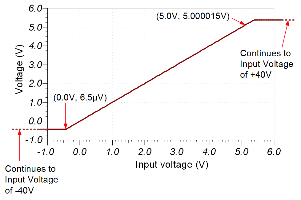
The following graph shows a linear output response for inputs from single-ended –40V to +40V. See Determining a SAR ADC’s Linear Range when using Operational Amplifiers for detailed theory on this subject. Note that the output range is intentionally limited to –0.42V to 5.38V using Schottky diodes to protect the ADS8860 device. Note that Schottky diodes are used because the low forward voltage drop (typically less than 0.3V) keeps the output limit very near the ADC supply voltages. The absolute maximum rating for the ADS8860 is –0.3V < Vin < REF +0.3V.
AC Transfer Characteristics
The bandwidth for this circuit is limited by the RC charge bucket circuit (Rfilt and Cfilt). The hand calculation and the simulated results compare well (hand calculation fc = 4.82MHz, simulated fc = 5.08MHz). See the Op Amp Bandwidth video series for more details on this subject.
Transient ADC Input Settling Simulation
The following simulation shows settling to a +5-V DC input signal with the OPA828 device. This type of simulation shows that the sample and hold kickback circuit is properly selected to drive ADS8860 at a 1-MSPS sampling rate and meets the desired ½ of a LSB (38.15µV). See the Introduction to SAR ADC Front-End Component Selection for detailed theory on this subject.
Noise Simulation
In this circuit example, the noise is dominated by the wide band amplifier noise so the resistors do not contribute significantly. Hence, the noise from the resistors is neglected in this calculation:
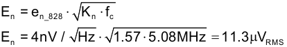
Note that calculated and simulated match well (simulated = 10.05µVRMS as in the following graph). See Calculating the Total Noise for ADC Systems for data converter noise.
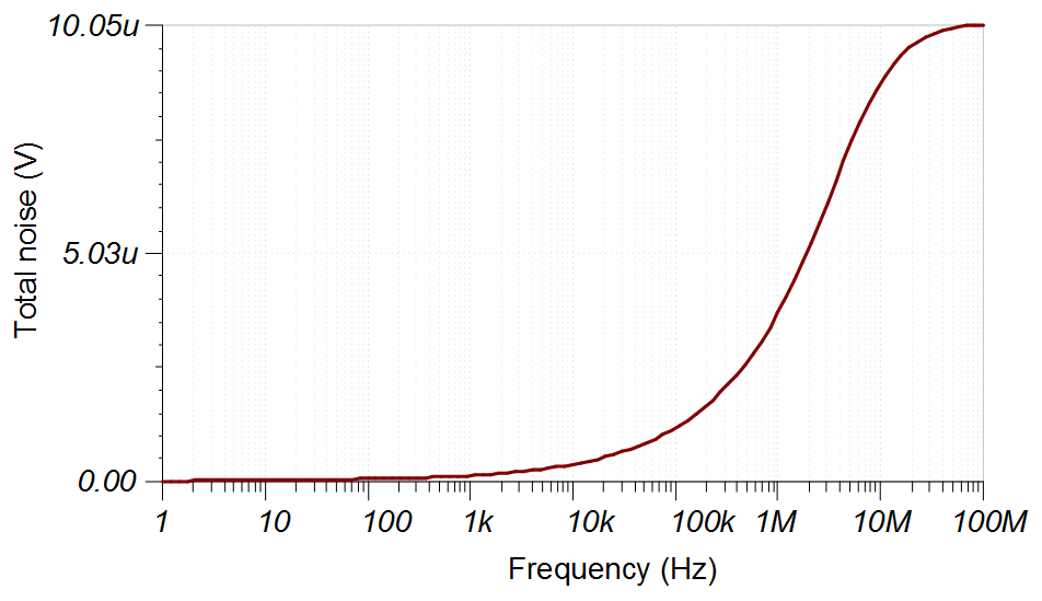
Stability
The following simulation shows a stability check for the performance-improved solution previously shown. This design has 69 degrees of phase margin which indicates that the circuit is very stable. Generally, the circuit which has more than 45 degrees of phase margin is considered to be stable. For more information on stability analysis check the Op Amps: Stability video series.
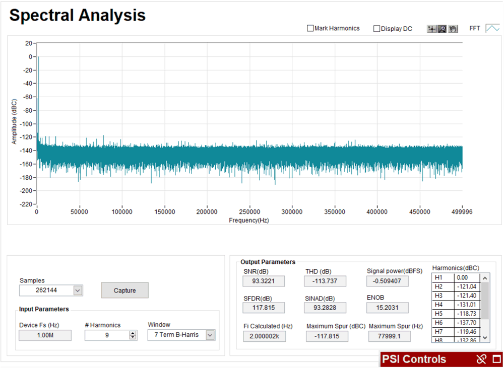
AC Performance Checked on Hardware
The following spectral analysis is measured using the PLABS-SAR-EVM-PDKTI Precision Labs SAR ADC Evaluation Module Performance Demonstration Kit (PDK). The AC performance including all the protection circuitry is better than the typical specifications in the ADS8860 16-bit, 1-MSPS, Serial Interface, Micropower, Miniature, Single-Ended Input, SAR Analog-to-Digital Converter data sheet (Measured SNR = 93.3dB, THD = –113.7dB, ADS8860 Typical: SNR = 92dB, THD = –108dB).
Design Featured Devices and Alternative Parts
| Device | Key Features | Link | Other Possible Devices |
|---|---|---|---|
| ADS8860 | 16-bit resolution, 1-MSPS sample rate, single-ended input, VREF input range 2.5V to 5.0V, SPI, SAR ADC | 16-bit, 1MSPS, 1-channel SAR ADC with single-ended input, SPI and daisy chain | Precision ADCs |
| ADS9224R | 16-bit, 3-MSPS, dual-channel, simultaneous-sampling SAR ADC with internal reference and enhanced SPI, SAR ADC | 16-bit, 3MSPS, dual-channel, simultaneous-sampling SAR ADC with internal reference and enhanced SPI | |
| ADS8168 | 16-bit, 1-MSPS, 8-channel, SAR ADC with VREF, VREF buffer and multiplexer, enhanced SPI SAR ADC | 16-bit, 1MSPS, 8-ch SAR ADC with VREF, VREF buffer and direct sensor interface | |
| OPA828 | 36-V, high-precision, low-noise, low-bias current, JFET- input operational amplifier | High-speed (45MHz and 150V/μs), 36V, low-noise (4nV/√Hz) RRO JFET operational amplifier | Operational amplifiers (op amps) |
Link to Key Files
Texas Instruments, SBAA372 sources files, tool support
Trademarks
All trademarks are the property of their respective owners.
IMPORTANT NOTICE AND DISCLAIMER
TI PROVIDES TECHNICAL AND RELIABILITY DATA (INCLUDING DATASHEETS), DESIGN RESOURCES (INCLUDING REFERENCE DESIGNS), APPLICATION OR OTHER DESIGN ADVICE, WEB TOOLS, SAFETY INFORMATION, AND OTHER RESOURCES “AS IS” AND WITH ALL FAULTS, AND DISCLAIMS ALL WARRANTIES, EXPRESS AND IMPLIED, INCLUDING WITHOUT LIMITATION ANY IMPLIED WARRANTIES OF MERCHANTABILITY, FITNESS FOR A PARTICULAR PURPOSE OR NON-INFRINGEMENT OF THIRD PARTY INTELLECTUAL PROPERTY RIGHTS.
These resources are intended for skilled developers designing with TI products. You are solely responsible for (1) selecting the appropriate TI products for your application, (2) designing, validating and testing your application, and (3) ensuring your application meets applicable standards, and any other safety, security, or other requirements. These resources are subject to change without notice. TI grants you permission to use these resources only for development of an application that uses the TI products described in the resource. Other reproduction and display of these resources is prohibited. No license is granted to any other TI intellectual property right or to any third party intellectual property right. TI disclaims responsibility for, and you will fully indemnify TI and its representatives against, any claims, damages, costs, losses, and liabilities arising out of your use of these resources.
TI’s products are provided subject to TI’s Terms of Sale (www.ti.com/legal/termsofsale.html) or other applicable terms available either on ti.com or provided in conjunction with such TI products. TI’s provision of these resources does not expand or otherwise alter TI’s applicable warranties or warranty disclaimers for TI products.
Mailing Address: Texas Instruments, Post Office Box 655303, Dallas, Texas 75265
Copyright © 2024, Texas Instruments Incorporated