-
TPS7A8300 2-A, 6-µVRMS, RF, LDO Voltage Regulator
- 1 Features
- 2 Applications
- 3 Description
- 4 Revision History
- 5 Pin Configurations and Functions
- 6 Specifications
-
7 Detailed Description
- 7.1 Overview
- 7.2 Functional Block Diagram
- 7.3
Feature Description
- 7.3.1 ANY-OUT Programmable Output Voltage
- 7.3.2 Adjustable Operation
- 7.3.3 ANY-OUT Operation
- 7.3.4 2-A LDO with an Internal Charge Pump
- 7.3.5 Low-Noise, 0.8-V Reference
- 7.3.6 Internal Protection Circuitry
- 7.3.7 Programmable Soft-Start
- 7.3.8 Power-Good Function
- 7.3.9 Integrated Resistance Network (ANY-OUT)
- 7.4 Device Functional Modes
- 8 Application and Implementation
- 9 Power-Supply Recommendations
- 10Layout
- 11Device and Documentation Support
- 12Mechanical, Packaging, and Orderable Information
- IMPORTANT NOTICE
TPS7A8300 2-A, 6-µVRMS, RF, LDO Voltage Regulator
1 Features
- Ultralow Dropout: 125 mV Maximum at 2 A
- Output Voltage Noise: 6 µVRMS
- Power-Supply Ripple Rejection:
- 40 dB at 1 MHz
- Input Voltage Range:
- Without BIAS: 1.4 V to 6.5 V
- With BIAS: 1.1 V to 6.5 V
- Two Output Voltage Modes:
- 1.0% Accuracy Over Line, Load, and Temperature
- Stable with a 22-µF Output Ceramic Capacitor
- Programmable Soft-Start Output
- Power-Good (PG) Output
- Available Packages:
2 Applications
- RF, IF Components: VCO, ADC, DAC, LVDS
- Wireless Infrastructure: SerDes, FPGA, DSP™
- Test and Measurement
- Instrumentation, Medical, and Audio
3 Description
The TPS7A8300 is a low-noise (6 µVRMS), low-dropout voltage regulator (LDO) capable of sourcing a 2-A load with only 125 mV of maximum dropout.
The TPS7A8300 output voltages are fully user-adjustable (up to 3.95 V) using a printed circuit board (PCB) layout without the need of external resistors, thus reducing overall component count. For higher output voltage applications, the device achieves output voltages up to 5 V with the use of external resistors. The device supports very low input voltages (down to 1.1 V) with the use of an additional BIAS rail.
With very high accuracy (1% over line, load, and temperature), remote sensing, and soft-start capabilities to reduce inrush current, the TPS7A8300 is ideal for powering high-current, low-voltage devices such as high-end microprocessors and field-programmable gate arrays (FPGAs).
The TPS7A8300 is designed to power-up noise-sensitive components in high-speed communication applications. The very low-noise, 6-µVRMS device output and high broad-bandwidth PSRR (40 dB at
1 MHz) minimizes phase noise and clock jitter in high-frequency signals. These features maximize performance of clocking devices, analog-to-digital converters (ADCs), and digital-to-analog converters (DACs).
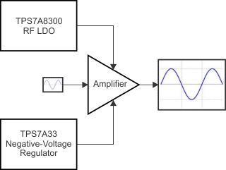
For applications where positive and negative low-noise rails are required, consider TI's TPS7A33 family of negative high-voltage, ultralow-noise linear regulators.
Device Information(1)
| PART NUMBER | PACKAGE | BODY SIZE (NOM) |
|---|---|---|
| TPS7A8300 | VQFN (20) | 5.00 mm × 5.00 mm |
| VQFN (20) | 3.50 mm × 3.50 mm |
- For all available packages, see the orderable addendum at the end of the datasheet.
4 Revision History
Changes from E Revision (August 2014) to F Revision
- Added title to page 1 graphic Go
- Updated ESD Ratings table to current standards Go
- Changed Figure 52: changed connection of EN pin Go
- Changed Enable (EN) and Undervoltage Lockout (UVLO) section: updated wording for better clarity on use of the Enable (EN) pin Go
Changes from D Revision (February 2013) to E Revision
- Changed format to meet latest data sheet standards; added new sections, and moved existing sectionsGo
- Changed first ANY-OUT sub-bullet of fifth Features bullet Go
- Changed eighth Features bullet: broke Soft-Start Output and PG Output into two separate Features bullets Go
- Changed first sentence of second paragraph in Description section Go
- Changed RGW and RGR drawings: removed spacing between number and unit in pins 5 to 7 and 9 to 11 Go
- Changed first row of Pin Functions table: deleted spacing between number and unit in pin namesGo
- Added capacitor value to BIAS pin description in Pin Functions tableGo
- Changed 87% to 89% in the PG pin description of the Pin Functions tableGo
- Changed thermal pad description in Pin Functions tableGo
- Changed conditions statements for Absolute Maximum Ratings and Recommended Operating Conditions tables Go
- Added Recommended Operating Conditions tableGo
- Changed the Typical Characteristics section: changed all curve titles and conditions Go
- Changed title of Figure 11 Go
- Added Overview section Go
- Changed second paragraph of Overview section: changed that can be groups, as follows to including Go
- Changed functional block diagram footnoteGo
- Added Feature Description sectionGo
- Changed adjustable version to adjustable configuration in first paragraph of Adjustable Operation section Go
- Changed Figure 51: removed right-hand side diagramGo
- Added Figure 52 Go
- Changed second sentence in Internal Charge Pump section Go
- Changed last sentence of UVLO sectionGo
- Changed oscillates to cycles in first paragraph of Thermal Protection sectionGo
- Changed first sentence of Programmable Soft-Start sectionGo
- Added Device Functional Modes sectionGo
- Added Application Information section Go
- Changed second paragraph of Noise sectionGo
- Added Typical Application section Go
- Added Figure 57 Go
Changes from C Revision (July 2013) to D Revision
- Changed document status from Mixed to Production DataGo
- Deleted footnote from second sub-bullet of last Features bulletGo
- Deleted footnote from RGR package drawingGo
- Changed GND pin description in Pin Descriptions tableGo
Changes from B Revision (July 2013) to C Revision
- Deleted PG Functionality sectionGo
- Changed Power-Good sectionGo
- Changed text in Feed-Forward Capacitor subsectionGo
Changes from A Revision (June 2013) to B Revision
- Changed from product preview to production data (mixed status)Go
Changes from * Revision (May 2013) to A Revision
- Changed product preview data sheetGo
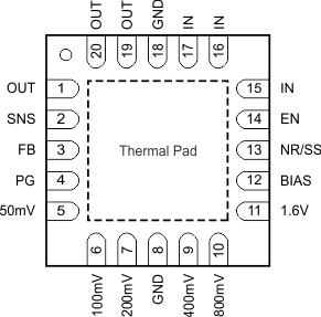
5 Pin Configurations and Functions
Pin Functions
| PIN | DESCRIPTION | ||
|---|---|---|---|
| NAME | NO. | I/O | |
| 50mV, 100mV, 200mV, 400mV, 800mV, 1.6V | 5, 6, 7, 9, 10, 11 | I | Output voltage setting pins. Connect these pins to ground or leave floating. Connecting these pins to ground increases the output voltage by the value of the pin name; multiple pins can be simultaneously connected to GND to select the desired output voltage. Leave these pins floating (open) when not in use. See the ANY-OUT Programmable Output Voltage section for more details. |
| BIAS | 12 | I | BIAS supply voltage pin for the use of 1.1 V ≤ VIN ≤ 1.4 V and to connect a 10-µF capacitor between this pin and ground. |
| EN | 14 | I | Enable pin. Driving this pin to logic high enables the device; driving this pin to logic low disables the device. See the Start-Up section for more details. |
| FB | 3 | I | Output voltage feedback pin connected to the error amplifier. Although not required, a 10-nF feed-forward capacitor from FB to OUT (as close to the device as possible) is recommended for low-noise applications to maximize ac performance. The use of a feed-forward capacitor may disrupt PG (power good) functionality. See the ANY-OUT Programmable Output Voltage and Adjustable Operation sections for more details. |
| GND | 8, 18 | — | Ground pin. These pins must be externally shorted for the RGR package option. |
| IN | 15-17 | I | Input supply voltage pin. A 10-μF input ceramic capacitor is required. See the Input and Output Capacitor Requirements (CIN and COUT) section for more details. |
| OUT | 1, 19, 20 | O | Regulated output pin. A 22-μF or larger ceramic capacitor is required for stability (a 10-μF minimum effective capacitance is required). See the Input and Output Capacitor Requirements (CIN and COUT) section for more details. |
| PG | 4 | O | Active-high power-good pin. An open-drain output indicates when the output voltage reaches 89% of the target. The use of a feed-forward capacitor may disrupt PG (power good) functionality. See the Power-Good Function section for more details. |
| SNS | 2 | I | Output voltage sense input pin. Connect this pin only if the ANY-OUT feature is used. See the ANY-OUT Programmable Output Voltage and Adjustable Operation sections for more details. |
| NR/SS | 13 | — | Noise-reduction and soft-start pin. Connecting an external capacitor between this pin and ground reduces reference voltage noise and also enables the soft-start function. Although not required, a capacitor is recommended for low-noise applications to connect a 10-nF capacitor from NR/SS to GND (as close to the device as possible) to maximize ac performance. See the Noise-Reduction and Soft-Start Capacitor (CNR/SS) section for more details. |
| Thermal Pad | Pad | — | Connect the thermal pad to a large-area ground plane. The thermal pad is internally connected to GND. |
6 Specifications
6.1 Absolute Maximum Ratings
over junction temperature range (unless otherwise noted) (1)| MIN | MAX | UNIT | ||
|---|---|---|---|---|
| Voltage | IN, BIAS, PG, EN | –0.3 | 7.0 | V |
| IN, BIAS, PG, EN (5% duty cycle) | –0.3 | 7.5 | ||
| SNS, OUT | –0.3 | VIN + 0.3 (2) | ||
| NR/SS, FB | –0.3 | 3.6 | ||
| 50mV, 100mV, 200mV, 400mV, 800mV, 1.6V | –0.3 | VOUT + 0.3 | ||
| Current | OUT | Internally limited | A | |
| PG (sink current into device) | 5 | mA | ||
| Operating junction temperature, TJ | –55 | 150 | °C | |
| Storage temperature, Tstg | –55 | 150 | °C | |
6.2 ESD Ratings
| VALUE | UNIT | |||
|---|---|---|---|---|
| V(ESD) | Electrostatic discharge | Human body model (HBM), per ANSI/ESDA/JEDEC JS-001(1) | ±2000 | V |
| Charged device model (CDM), per JEDEC specification JESD22-C101(2) | ±500 | |||
6.3 Recommended Operating Conditions
over junction temperature range (unless otherwise noted)| MIN | MAX | UNIT | ||
|---|---|---|---|---|
| VIN | Input supply voltage range | 1.1 | 6.5 | V |
| VBIAS | Bias supply voltage range(1) | 3.0 | 6.5 | V |
| IOUT | Output current | 0 | 2 | A |
| TJ | Operating junction temperature | –40 | 125 | °C |
6.4 Thermal Information
| THERMAL METRIC(1) | TPS7A8300 | UNIT | ||
|---|---|---|---|---|
| RGW (QFN) | RGR (QFN) | |||
| 20 PINS | 20 PINS | |||
| RθJA | Junction-to-ambient thermal resistance | 33.6 | 35.4 | °C/W |
| RθJC(top) | Junction-to-case (top) thermal resistance | 30.0 | 47.6 | °C/W |
| RθJB | Junction-to-board thermal resistance | 14.0 | 12.3 | °C/W |
| ψJT | Junction-to-top characterization parameter | 0.2 | 0.5 | °C/W |
| ψJB | Junction-to-board characterization parameter | 14.0 | 12.4 | °C/W |
| RθJC(bot) | Junction-to-case (bottom) thermal resistance | 1.6 | 1.0 | °C/W |
6.5 Electrical Characteristics
Over operating temperature range (TJ = –40°C to 125°C), {1.1 V ≤ VIN < 1.4 V and 3.0 V ≤ VBIAS ≤ 6.5 V} or {VIN ≥ 1.4 V and VBIAS open}(1), VIN ≥ VOUT(TARGET) + 0.3 V(2), VOUT(TARGET) = 0.8 V, OUT connected to 50 Ω to GND(3), VEN = 1.1 V, COUT =22 μF, CNR/SS = 0 nF, CFF = 0 nF, and PG pin pulled up to VIN with 100 kΩ, unless otherwise noted.
Typical values are at TJ = 25°C.
| PARAMETER | TEST CONDITIONS | MIN | TYP | MAX | UNIT | ||
|---|---|---|---|---|---|---|---|
| VIN | Input supply voltage range | 1.1 | 6.5 | V | |||
| VBIAS | Bias supply voltage range(1) | 3.0 | 6.5 | V | |||
| V(REF) | Reference voltage | V(REF) = V(FB) = V(NR/SS) | 0.8 | V | |||
| VUVLO1(IN) | Input supply UVLO with BIAS | VIN increasing | 1.02 | 1.085 | V | ||
| VHYS1(IN) | VUVLO1(IN) hysteresis | 320 | mV | ||||
| VUVLO2(IN) | Input supply UVLO without BIAS | VIN increasing | 1.31 | 1.39 | V | ||
| VHYS2(IN) | VUVLO2(IN) hysteresis | 253 | mV | ||||
| VUVLO(BIAS) | Bias supply UVLO | VBIAS increasing | 2.83 | 2.9 | V | ||
| VHYS(BIAS) | VUVLO(BIAS) hysteresis | 290 | mV | ||||
| VOUT | Output voltage range | Using voltage setting pins (50mV, 100mV, 200mV, 400mV, 800mV, and 1.6V) | 0.8 – 1.0% | 3.95 + 1.0% | V | ||
| Using external resistors | 0.8 – 1.0% | 5.0 + 1.0% | |||||
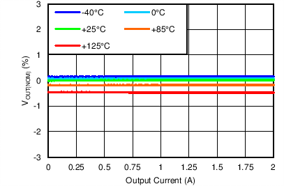
| Output voltage accuracy(4)(5) | 0.8 V ≤ VOUT ≤ 5 V, 5 mA ≤ IOUT ≤ 2 A | –1.0% | 1.0% | ||||
| VIN = 1.5 V, VOUT = 1.2 V, 5 mA ≤ IOUT ≤ 1.2 A | –1.0% | 1.0% | |||||
| ΔVO(ΔVI) | Line regulation | IOUT = 5 mA, 1.4 V ≤ VIN ≤ 6.5 V | 0.003 | %/V | |||
| ΔVO(ΔIO) | Load regulation | 5 mA ≤ IOUT ≤ 2 A | 0.0001 | %/A | |||
| V(DO) | Dropout voltage | VIN ≥ 1.4 V and VBIAS open, 0.8 V ≤ VOUT ≤ 5.0 V, IOUT = 2 A, VFB = 0.8 V – 3% |
200 | mV | |||
| VIN = 1.1 V, VBIAS = 5.0 V, VOUT(TARGET) = 0.8 V, IOUT = 2 A, VFB = 0.8 V – 3% |
125 | ||||||
| I(LIM) | Output current limit | VOUT forced at 0.9 × VOUT(TARGET), VIN = VOUT(TARGET) + 300 mV |
2.1 | 3.4 | 4.2 | A | |
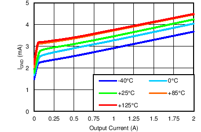
| I(GND) | GND pin current | Minimum load, VIN = 6.5 V, no VBIAS supply, IOUT = 5 mA |
2.8 | 4 | mA | ||
| Maximum load, VIN = 1.4 V, no VBIAS supply, IOUT = 2 A |
3.7 | 5 | |||||
| Shutdown, PG = (open), VIN = 6.5 V, no VBIAS supply, V(EN) = 0.5 V |
2.5 | μA | |||||
| I(EN) | EN pin current | VIN = 6.5 V, no VBIAS supply, V(EN) = 0 V and 6.5 V | –0.1 | 0.1 | μA | ||
| I(BIAS) | BIAS pin current | VIN = 1.1 V, VBIAS = 6.5 V, VOUT(TARGET) = 0.8 V, IOUT = 2 A |
2.3 | 3.5 | mA | ||
| VIL(EN) | EN pin low-level input voltage (disable device) | 0 | 0.5 | V | |||
| VIH(EN) | EN pin high-level input voltage (enable device) | 1.1 | 6.5 | V | |||
| VIT(PG) | PG pin threshold | For the direction PG↓ with decreasing VOUT | 0.82 VOUT | 0.872 VOUT | 0.93 VOUT | V | |
| Vhys(PG) | PG pin hysteresis | For PG↑ | 0.02 VOUT | V | |||
| VOL(PG) | PG pin low-level output voltage | VOUT < VIT(PG), IPG = –1 mA (current into device) | 0.4 | V | |||
| Ilkg(PG) | PG pin leakage current | VOUT > VIT(PG), V(PG) = 6.5 V | 1 | μA | |||
| I(NR/SS) | NR/SS pin charging current | VNR/SS = GND, VIN = 6.5 V | 4.0 | 6.2 | 9.0 | μA | |
| IFB | FB pin leakage current | VIN = 6.5 V | –100 | 100 | nA | ||
| PSRR | Power-supply ripple rejection | f = 1 MHz, VIN = 3.8 V, VOUT = 3.3 V, IOUT = 2 A, CNR/SS = 10 nF, CFF = 10 nF |
40 | dB | |||
| Vn | Output noise voltage | BW = 10 Hz to 100 kHz, VIN = 1.4 V, VOUT = 0.8 V, IOUT = 1.5 A, CNR/SS = 10 nF, CFF = 10 nF |
6 | μVRMS | |||
| Tsd | Thermal shutdown temperature | Shutdown, temperature increasing | 160 | °C | |||
| Reset, temperature decreasing | 140 | ||||||
| TJ | Operating junction temperature | –40 | 125 | °C | |||
6.6 Typical Characteristics
At TJ = 25°C, {1.1 V ≤ VIN < 1.4 V and 3.0 V ≤ VBIAS ≤ 6.5 V} or {VIN ≥ 1.4 V and VBIAS open}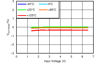
| VOUT(TARGET) = 0.8 V, IOUT = 5 mA, VBIAS = Open |
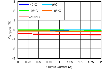
| VOUT(TARGET) = 0.8 V, VIN = 1.4 V, VBIAS = Open |
No BIAS Load Regulation
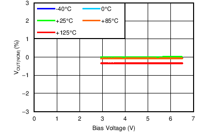
| VOUT(TARGET) = 0.8 V, VIN = 1.1 V, IOUT = 5 mA |
Line Regulation
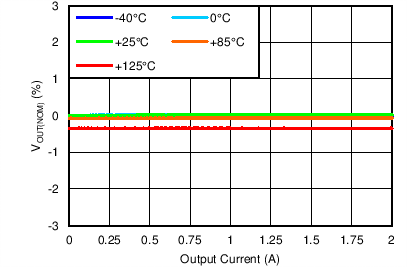
| VOUT(TARGET) = 0.8 V, VIN = 1.1 V, VBIAS = 6.5 V |
Maximum BIAS Load Regulation
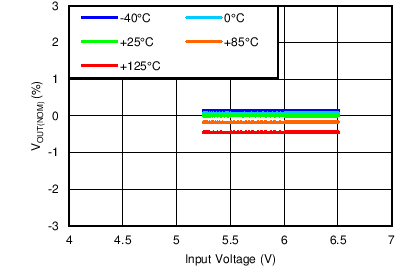
| VOUT(TARGET) = 5 V, IOUT = 5 mA, VBIAS = Open |
Line Regulation
| VIN = 5.5 V, ANY-OUT, VBIAS = Open, |
| VBIAS = Open, IOUT = 2 A, ANY-OUT |
| VIN = 1.1 V, ANY-OUT, IOUT = 2 A |
| VOUT(TARGET) = 0.8 V, IOUT = 5 mA, VIN = 1.1 V |
Quiescent Current vs Bias Voltage
| VOUT(TARGET) = 0.8 V, VIN = 1.1 V, VBIAS = 3 V |
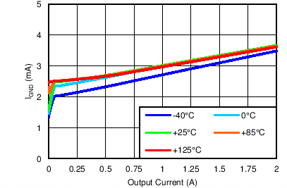
Quiescent Current vs Output Current
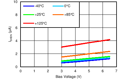
| VOUT(TARGET) = 0.8 V, VIN = 1.1 V |
Shutdown Current vs Bias Voltage
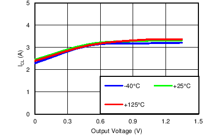
| VIN = 1.8 V, ANY-OUT, VBIAS = Open, VOUT(TARGET) = 1.5 V |
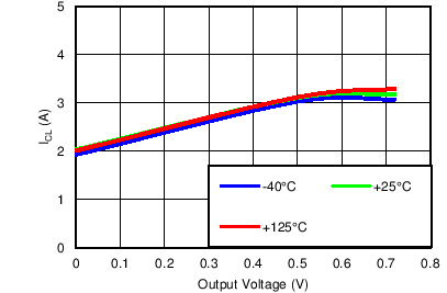
| VOUT(TARGET) = 0.8 V, VIN = 1.1 V, VBIAS = 3 V |
Current Limit vs Output Voltage
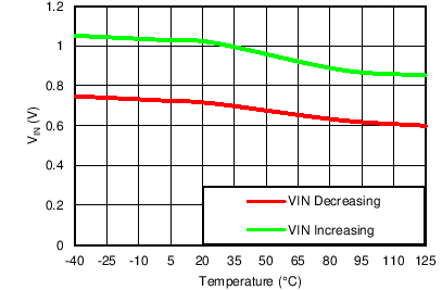
| VOUT(TARGET) = 0.8 V, VBIAS = 3.0 V |
Input UVLO Threshold vs Temperature
| VOUT(TARGET) = 0.8 V, VIN = 1.1 V |
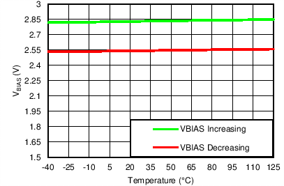
UVLO Threshold vs Temperature
| VOUT(TARGET) = 0.8 V, VIN = 6.5 V, VBIAS = Open |
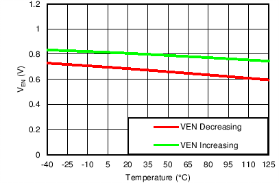
Enable Threshold vs Temperature
| VIN = 6.5 V, VOUT(TARGET) = 0.8 V, VBIAS = Open |
| VOUT(TARGET) = 0.8 V, VIN = 6.5 V, VBIAS = Open |
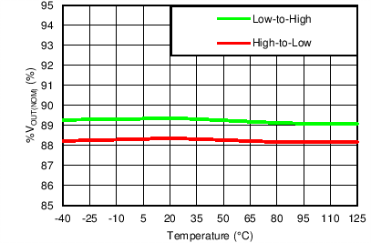
PG Threshold vs Temperature
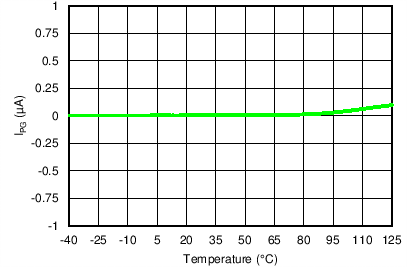
| VOUT(TARGET) = 0.8 V, VIN = VPG = 6.5 V, VBIAS = Open | ||
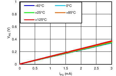
PG Current vs Temperature
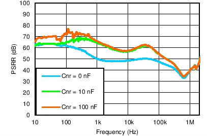
| VOUT(TARGET) = 3.3 V, ANY-OUT, VIN = VEN = 3.8 V, VBIAS = Open, IOUT = 1.5 A, COUT = 22 µF, CFF = 10 nF |
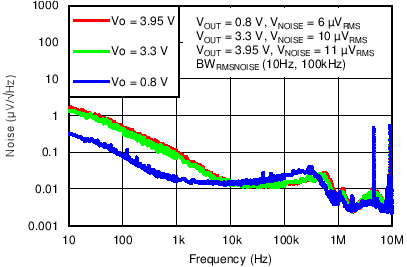
| VIN = VOUT(TARGET) + 0.5 V, ANY-OUT, VBIAS = Open, IOUT = 1.5 A, COUT = 22 µF, CNR/SS = CFF = 10 nF |
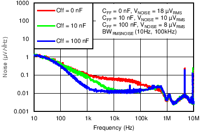
| VIN = 3.8 V, VOUT(TARGET) = 3.3 V, ANY-OUT, VBIAS = Open, IOUT = 1.5 A, COUT = 22 µF, CNR/SS = 10 nF |
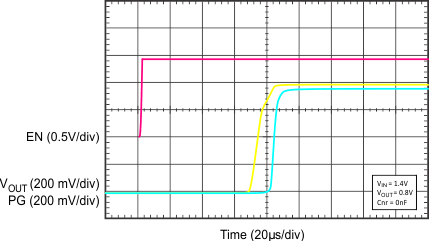
| VIN = 1.4 V, VOUT = 0.8 V, CNR/SS = 0 nF |
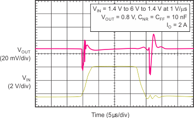
| VIN = 1.4 V to 6 V to 1.4 V at 1 V/µs, VOUT = 0.8 V, IOUT = 2 A, CNR/SS = CFF = 10 nF |
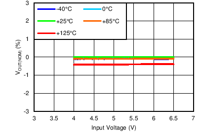
| VOUT(TARGET) = 3.95 V, IOUT = 5 mA, VBIAS = Open |
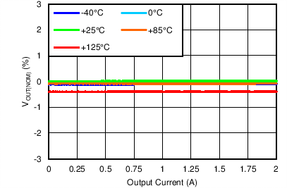
| VOUT(TARGET) = 3.95 V, VIN = 4.25 V, VBIAS = Open |

| VOUT(TARGET) = 0.8 V, VIN = 1.1 V, VBIAS = 3 V |
BIAS Load Regulation
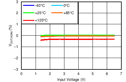
| VOUT(TARGET) = 0.8 V, IOUT = 5 mA, VBIAS = Open |
Line Regulation
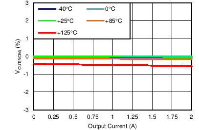
| VOUT(TARGET) = 0.8 V, VIN = 1.4 V, VBIAS = Open | ||
No BIAS Load Regulation
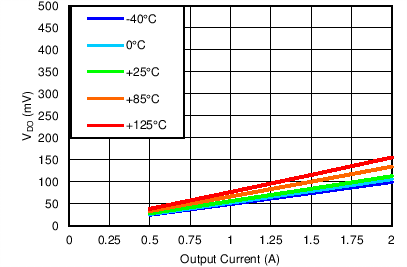
| VIN = 1.4 V, ANY-OUT, VBIAS = Open, No BIAS |
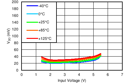
| VBIAS = Open, IOUT = 0.5 A, ANY-OUT |
| VIN = 1.1 V, ANY-OUT, IOUT = 0.5 A |
| VOUT(TARGET) = 0.8 V, IOUT = 5 mA, VBIAS = Open |
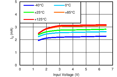
Quiescent Current vs Input Voltage
| VOUT(TARGET) = 0.8 V, VIN = 1.4 V, VBIAS = Open |
| VOUT(TARGET) = 0.8 V, VBIAS = Open |
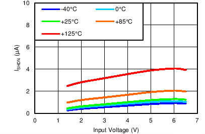
Shutdown Current vs Input Voltage
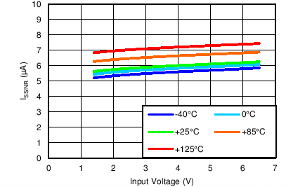
| VOUT(TARGET) = 0.8 V, VBIAS = Open |
Soft-Start Current vs Input Voltage
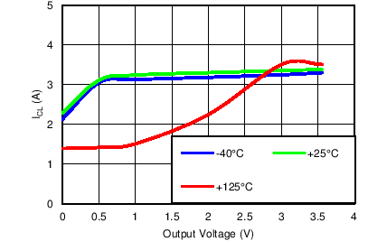
| VOUT(TARGET) = 3.95 V, VIN = 4.25 V, VBIAS = Open |
Current Limit vs Output Voltage
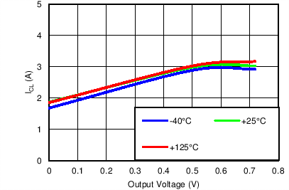
| VOUT(TARGET) = 0.8 V, VIN = 1.1 V, VBIAS = 6.5 V |
Maximum BIAS Current Limit vs Output Voltage
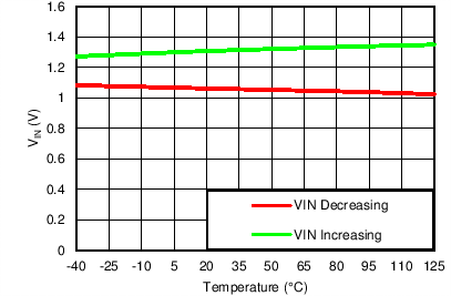
| VOUT(TARGET) = 0.8 V, VBIAS = Open |
Input UVLO Threshold vs Temperature
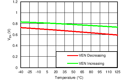
| VOUT(TARGET) = 0.8 V, VIN = 1.4 V, VBIAS = Open |
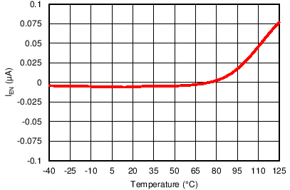
| VOUT(TARGET) = 0.8 V, VIN = VEN = 6.5 V, VBIAS = Open |
Enable Current vs Temperature
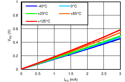
| VOUT(TARGET) = 0.8 V, VIN = 1.4 V, VBIAS = Open |
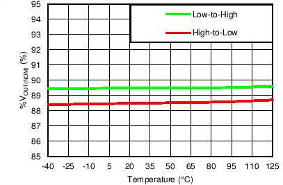
| VOUT(TARGET) = 0.8 V, VIN = 1.4 V, VBIAS = Open |
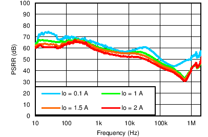
| VOUT(TARGET) = 3.3 V, ANY-OUT, VIN = VEN = 3.8 V, VBIAS = Open, COUT = 22 µF, CNR/SS = CFF = 10 nF |
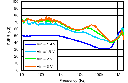
| VOUT(TARGET) = 1.2 V, ANY-OUT, VBIAS = Open, IOUT = 1.5 A, COUT = 22 µF, CNR/SS = CFF = 10 nF |
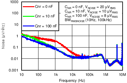
| VIN = 3.8 V, VOUT(TARGET) = 3.3 V, ANY-OUT, VBIAS = Open, IOUT = 1.5 A, COUT = 22 µF, CFF = 10 nF |
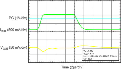
| VIN = 3.85 V, VOUT = 3.3 V, IOUT = 100 mA to 1 A to 100 mA at 1 A/µs, CO = 22 µF |
||
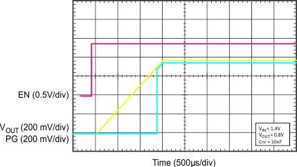
| VIN = 1.4 V, VOUT = 0.8 V, CNR/SS = 10 nF |
7 Detailed Description
7.1 Overview
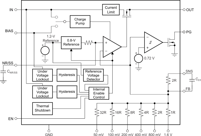
The TPS7A8300 is a low-noise, high PSRR, low-dropout regulator capable of sourcing a 2-A load with only
125 mV of maximum dropout. The TPS7A8300 can operate down to 1.1-V input voltage and 0.8-V output voltage. This combination of low noise, high PSRR, and low output voltage makes the device an ideal low dropout (LDO) regulator to power a multitude of loads from noise-sensitive communication components in high-speed communication applications to high-end microprocessors or field-programmable gate arrays (FPGAs).
The TPS7A8300 block diagram contains several features, including:
- A 2-A, low-dropout regulator with an internal charge pump,
- Low-noise, 0.8-V reference,
- Internal protection circuitry, such as undervoltage lockout (UVLO), foldback current limit, and thermal shutdown,
- Programmable soft-start,
- Power-good output, and
- An integrated resistance network (ANY-OUT) with a 50-mV minimum resolution.
7.3 Feature Description
7.3.1 ANY-OUT Programmable Output Voltage
The TPS7A8300 does not require external resistors to set output voltage, which is typical of adjustable low-dropout voltage regulators (LDOs). However, the TPS7A8300 uses pins 5, 6, 7, 9, 10, and 11 to program the regulated output voltage. Each pin is either connected to ground (active) or left open (floating). ANY-OUT programming is set by Equation 1 as the sum of the internal reference voltage (VREF = 0.8 V) plus the accumulated sum of the respective voltages assigned to each active pin; that is, 50mV (pin 5), 100mV (pin 6), 200mV (pin 7), 400mV (pin 9), 800mV (pin 10), or 1.6V (pin 11). Table 1 summarizes these voltage values associated with each active pin setting for reference. By leaving all program pins open, or floating, the output is thereby programmed to the minimum possible output voltage equal to VREF.

Table 1. ANY-OUT Programmable Output Voltage
| ANY-OUT PROGRAM PINS (Active Low) | ADDITIVE OUTPUT VOLTAGE LEVEL |
|---|---|
| Pin 5 (50mV) | 50 mV |
| Pin 6 (100mV) | 100 mV |
| Pin 7 (200mV) | 200 mV |
| Pin 9 (400mV) | 400 mV |
| Pin 10 (800mV) | 800 mV |
| Pin 11 (1.6V) | 1.6 V |
Table 2 provides a full list of target output voltages and corresponding pin settings. The voltage setting pins have a binary weight; therefore, the output voltage can be programmed to any value from 0.8 V to 3.95 V in 50-mV steps.
There are several alternative ways to set the output voltage. The program pins can be driven using external general-purpose input/output pins (GPIOs), manually connected to ground using 0-Ω resistors (or left open), or hardwired by the given layout of the printed circuit board (PCB) to set the ANY-OUT voltage.
NOTE
For output voltages greater than 3.95 V, use a traditional adjustable configuration (see the Adjustable Operation section).
Table 2. User-Configurable Output Voltage Settings
| VOUT(TARGET)
(V) |
50mV | 100mV | 200mV | 400mV | 800mV | 1.6V | VOUT(TARGET)
(V) |
50mV | 100mV | 200mV | 400mV | 800mV | 1.6V | |
|---|---|---|---|---|---|---|---|---|---|---|---|---|---|---|
| 0.80 | Open | Open | Open | Open | Open | Open | 2.40 | Open | Open | Open | Open | Open | GND | |
| 0.85 | GND | Open | Open | Open | Open | Open | 2.45 | GND | Open | Open | Open | Open | GND | |
| 0.90 | Open | GND | Open | Open | Open | Open | 2.50 | Open | GND | Open | Open | Open | GND | |
| 0.95 | GND | GND | Open | Open | Open | Open | 2.55 | GND | GND | Open | Open | Open | GND | |
| 1.00 | Open | Open | GND | Open | Open | Open | 2.60 | Open | Open | GND | Open | Open | GND | |
| 1.05 | GND | Open | GND | Open | Open | Open | 2.65 | GND | Open | GND | Open | Open | GND | |
| 1.10 | Open | GND | GND | Open | Open | Open | 2.70 | Open | GND | GND | Open | Open | GND | |
| 1.15 | GND | GND | GND | Open | Open | Open | 2.75 | GND | GND | GND | Open | Open | GND | |
| 1.20 | Open | Open | Open | GND | Open | Open | 2.80 | Open | Open | Open | GND | Open | GND | |
| 1.25 | GND | Open | Open | GND | Open | Open | 2.85 | GND | Open | Open | GND | Open | GND | |
| 1.30 | Open | GND | Open | GND | Open | Open | 2.90 | Open | GND | Open | GND | Open | GND | |
| 1.35 | GND | GND | Open | GND | Open | Open | 2.95 | GND | GND | Open | GND | Open | GND | |
| 1.40 | Open | Open | GND | GND | Open | Open | 3.00 | Open | Open | GND | GND | Open | GND | |
| 1.45 | GND | Open | GND | GND | Open | Open | 3.05 | GND | Open | GND | GND | Open | GND | |
| 1.50 | Open | GND | GND | GND | Open | Open | 3.10 | Open | GND | GND | GND | Open | GND | |
| 1.55 | GND | GND | GND | GND | Open | Open | 3.15 | GND | GND | GND | GND | Open | GND | |
| 1.60 | Open | Open | Open | Open | GND | Open | 3.20 | Open | Open | Open | Open | GND | GND | |
| 1.65 | GND | Open | Open | Open | GND | Open | 3.25 | GND | Open | Open | Open | GND | GND | |
| 1.70 | Open | GND | Open | Open | GND | Open | 3.30 | Open | GND | Open | Open | GND | GND | |
| 1.75 | GND | GND | Open | Open | GND | Open | 3.35 | GND | GND | Open | Open | GND | GND | |
| 1.80 | Open | Open | GND | Open | GND | Open | 3.40 | Open | Open | GND | Open | GND | GND | |
| 1.85 | GND | Open | GND | Open | GND | Open | 3.45 | GND | Open | GND | Open | GND | GND | |
| 1.90 | Open | GND | GND | Open | GND | Open | 3.50 | Open | GND | GND | Open | GND | GND | |
| 1.95 | GND | GND | GND | Open | GND | Open | 3.55 | GND | GND | GND | Open | GND | GND | |
| 2.00 | Open | Open | Open | GND | GND | Open | 3.60 | Open | Open | Open | GND | GND | GND | |
| 2.05 | GND | Open | Open | GND | GND | Open | 3.65 | GND | Open | Open | GND | GND | GND | |
| 2.10 | Open | GND | Open | GND | GND | Open | 3.70 | Open | GND | Open | GND | GND | GND | |
| 2.15 | GND | GND | Open | GND | GND | Open | 3.75 | GND | GND | Open | GND | GND | GND | |
| 2.20 | Open | Open | GND | GND | GND | Open | 3.80 | Open | Open | GND | GND | GND | GND | |
| 2.25 | GND | Open | GND | GND | GND | Open | 3.85 | GND | Open | GND | GND | GND | GND | |
| 2.30 | Open | GND | GND | GND | GND | Open | 3.90 | Open | GND | GND | GND | GND | GND | |
| 2.35 | GND | GND | GND | GND | GND | Open | 3.95 | GND | GND | GND | GND | GND | GND |
7.3.2 Adjustable Operation
The TPS7A8300 can be used either with the internal ANY-OUT network or using external resistors. Using the ANY-OUT network allows the TPS7A8300 to be programmed from 0.8 V to 3.95 V. To extend this range of output voltage operation to 5.0 V, external resistors must be used. This configuration is referred to as the adjustable configuration of the TPS7A8300 throughout this document. Regardless whether the internal resistor network or whether external resistors are used, the nominal output voltage of the device is set by two resistors, as shown in Figure 50. Using an internal resistor ensures a 1% matching and minimizes both the number of external components and layout footprint.
 Figure 50. Adjustable Operation for Maximum AC Performance
R1 and R2 can be calculated for any output voltage range using Equation 2. This resistive network must provide a current equal to or greater than 5 μA for optimum noise performance.

If greater voltage accuracy is required, take into account the output voltage offset contributions resulting from the feedback pin current (IFB) and use 0.1% tolerance resistors.
Table 3 shows the resistor combination required to achieve a few of the most common rails using commercially-available, 0.1%-tolerance resistors to maximize nominal voltage accuracy while abiding to the formula shown in Equation 2.
Table 3. Recommended Feedback-Resistor Values
| VOUT(TARGET)
(V) |
FEEDBACK RESISTOR VALUES (1) | |
|---|---|---|
| R1 (kΩ) | R2 (kΩ) | |
| 1.00 | 2.55 | 10.2 |
| 1.20 | 5.9 | 11.8 |
| 1.50 | 9.31 | 10.7 |
| 1.80 | 18.7 | 15 |
| 1.90 | 15.8 | 11.5 |
| 2.50 | 24.3 | 11.5 |
| 3.00 | 31.6 | 11.5 |
| 3.30 | 35.7 | 11.5 |
| 5.00 | 105 | 20 |
7.3.3 ANY-OUT Operation
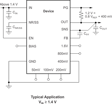
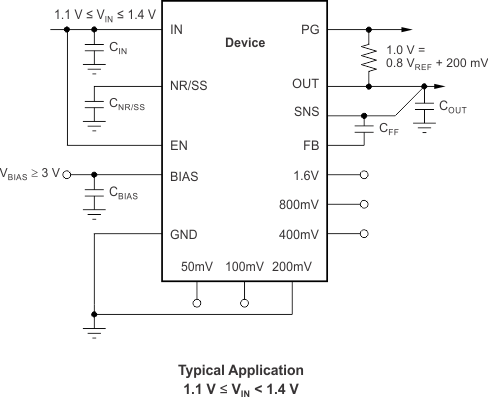
Considering the use of the ANY-OUT internal network (where the unit resistance of 1R is equal to 6.05 kΩ) the output voltage is set by grounding the appropriate control pins, as shown in Figure 51. When grounded, all control pins add a specific voltage on top of the internal reference voltage (VREF = 0.8 V). The output voltage can be equated with Equation 4. Figure 51 and Figure 52 show a 1.2-V and 1-V output voltage, respectively, that provide an example of the circuit usage with and without BIAS voltage. These schematics are described in more detail in the Typical Application section.
7.3.4 2-A LDO with an Internal Charge Pump
The TPS7A8300 can be used either with the internal resistor network provided, or with the external component as a traditional adjustable LDO. Regardless of the implementation, the TPS7A8300 provides excellent regulation to 1% accuracy, excellent dropout voltage, and high output current capability.
If the input voltage is below 1.4 V, an external BIAS voltage must be supplied to maintain the dropout characteristics. The input voltage or the BIAS voltage is fed through to a internal charge pump to power the internal error amplifier providing the regulation.
7.3.4.1 Dropout Voltage (VDO)
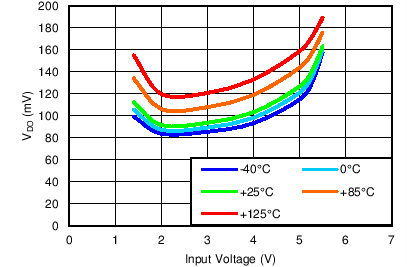
Generally speaking, the dropout voltage often refers to the voltage difference between the input and output voltage (VDO = VIN – VOUT). However, in the , VDO is defined as the VIN – VOUT voltage at the rated current (IRATED), where the main current pass-FET is fully on in the ohmic region of operation and is characterized by the classic RDS(ON) of the FET. VDO indirectly specifies a minimum input voltage above the nominal programmed output voltage at which the output voltage is expected to remain within its accuracy boundary. If the input falls below this VDO limit (VIN < VOUT + VDO), then the output voltage decreases in order to follow the input voltage.
Dropout voltage is always determined by the RDS(ON) of the main pass-FET. Therefore, if the LDO operates below the rated current, then the VDO for that current scales accordingly. The RDS(ON) for the TPS7A8300 can be calculated using Equation 5:

7.3.4.2 Output Voltage Accuracy
Output voltage accuracy specifies minimum and maximum output voltage error, relative to the expected nominal output voltage stated as a percent. This accuracy error includes the errors introduced by the internal reference and the load and line regulation across the full range of rated load and line operating conditions over temperature, unless otherwise specified by the Electrical Characteristics. Output voltage accuracy also accounts for all variations between manufacturing lots.
7.3.4.3 Internal Charge Pump
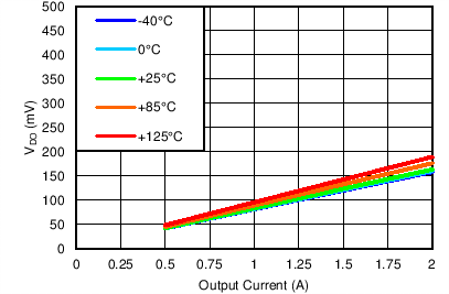
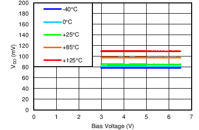
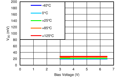
The internal charge pump ensures proper operation without requiring an external BIAS voltage down to +1.4-V input voltage. Below a 1.4-V input voltage, a BIAS input voltage between 3.0 V and 6.5 V is required. Dropout plots in the ohmic region of the pass-FET are illustrated in the Typical Characteristics section (Figure 12 through Figure 17).
7.3.5 Low-Noise, 0.8-V Reference
The TPS7A8300 includes a low-noise reference ensuring minimal noise during operation because the internal reference is normally the dominant term in noise analysis. Further noise reduction can be achieved using the NR/SS pin and by adding an external CFF between the SNS pin and the FB pin.
7.3.6 Internal Protection Circuitry
7.3.6.1 Undervoltage Lockout (UVLO)
The undervoltage lockout (UVLO) circuit monitors the input and bias voltage (VIN and VBIAS, respectively) to prevent the device from turning on before VIN and VBIAS rise above the lockout voltage. The UVLO circuit also causes a shutdown when VIN and VBIAS fall below the lockout voltage.
7.3.6.2 Internal Current Limit (I(LIM))
The internal current limit circuit is used to protect the LDO against high-load current faults or shorting events. The LDO is not designed to operate in a steady-state current limit. During a current-limit event, the LDO sources constant current. Therefore, the output voltage falls when load impedance decreases. Note also that if a current limit occurs and the resulting output voltage is low, excessive power may be dissipated across the LDO, resulting in a thermal shutdown of the output.
A foldback feature limits the short-circuit current to protect the regulator from damage under all load conditions. If OUT is forced below 0 V before EN goes high and the load current required exceeds the foldback current limit, the device does not start up. In applications that function with both a positive and negative voltage supply, there are several ways to ensure proper start-up:
- Enable the TPS7A8300 first and disable the device last.
- Delaying the EN voltage with respect to the IN voltage allows the internal pull-down resistor to discharge any residual voltage at OUT. If a faster discharge rate is required, use an external resistor from OUT to GND.
7.3.6.3 Thermal Protection
The TPS7A8300 contains a thermal shutdown protection circuit to turn off the output current when excessive heat is dissipated in the LDO. Thermal shutdown occurs when the thermal junction temperature (TJ) of the main pass-FET exceeds 160°C (typical). Thermal shutdown hysteresis assures that the LDO resets again (turns on) when the temperature falls to 140°C (typical). The thermal time-constant of the semiconductor die is fairly short, and thus the output cycles on and off at a high rate when thermal shutdown is reached until the power dissipation is reduced.
For reliable operation, limit the junction temperature to a maximum of 125°C. To estimate the thermal margin in a given layout, increase the ambient temperature until the thermal protection shutdown is triggered using worst-case load and highest input voltage conditions. For good reliability, thermal shutdown occurs at least 45°C above the maximum expected ambient temperature condition for the application. This configuration produces a worst-case junction temperature of 125°C at the highest expected ambient temperature and worst-case load.
The internal protection circuitry of the TPS7A8300 is designed to protect against thermal overload conditions. The circuitry is not intended to replace proper heat sinking. Continuously running the TPS7A8300 into thermal shutdown degrades device reliability.
7.3.7 Programmable Soft-Start
Soft-start refers to the ramp-up characteristic of the output voltage during LDO turn-on after EN and UVLO exceed the respective threshold voltage. The noise-reduction capacitor (CNR/SS) serves a dual purpose of both governing output noise reduction and programming the soft-start ramp during turn-on. See the Application and Implementation section on implementing a soft-start.
7.3.8 Power-Good Function
The TPS7A8300 has a power-good function that works by toggling the state of the PG output pin. When the output voltage falls below the PG threshold voltage (VIT(PG)), the PG pin open-drain output engages (low impedance to GND). When the output voltage exceeds the VIT(PG) threshold by an amount greater than VHYS(PG), the PG pin becomes high-impedance. By connecting a pull-up resistor to an external supply, any downstream device can receive PG as a logic signal. Make sure that the external pull-up supply voltage results in a valid logic signal for the receiving device or devices. Use a pull-up resistor from 10 kΩ to 100 kΩ for best results.
When employing the feed-forward capacitor (CFF), the turn-on time-constant for the LDO is increased and the power-good output time-constant stays the same, resulting in an invalid status of the LDO. To avoid this issue and receive a valid PG output, ensure that the time-constant of both the LDO and the power-good output match. For more details, see application report, Pros and Cons of Using a Feed-Forward Capacitor with a Low Dropout Regulator, SBVA042.
7.3.9 Integrated Resistance Network (ANY-OUT)
An internal resistance network is provided allowing the TPS7A8300 output voltage to be programmed easily between 0.8 V to 3.95 V with a 50-mV step.
7.4 Device Functional Modes
7.4.1 Operation with 1.1 V > VIN > 1.4 V
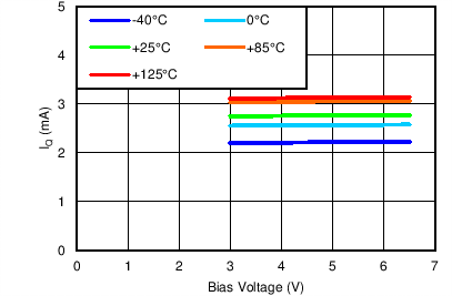
The TPS7A8300 requires a bias voltage on the BIAS pin ≥ 3.0 V if the high-current input supply voltage is between 1.1 to 1.4 V. The bias voltage pin consumes 2.3 mA, nominally.
7.4.2 Operation with 1.4 V ≥ VIN > 6.5 V
If the input voltage is equal to, or exceeds 1.4 V, no bias voltage is necessary. The device is automatically selected to be powered from the IN pin in this condition and the BIAS pin can be left floating.
7.4.3 Disabled
If the voltage on the EN pin is less than 0.5 V, the device is disabled and the output is high impedance. The output impedance of the LDO is then set by the gain setting resistors if a path to GND is provided between OUT and GND. Raising EN above 1.1 V (maximum) initiates the startup sequence of the device. In this state, quiescent current does not exceed 2.5 µA.
8 Application and Implementation
NOTE
Information in the following applications sections is not part of the TI component specification, and TI does not warrant its accuracy or completeness. TI’s customers are responsible for determining suitability of components for their purposes. Customers should validate and test their design implementation to confirm system functionality.
8.1 Application Information
The TPS7A8300 is a linear voltage regulator operating from 1.1 V to 6.5 V on the input and regulates voltages between 0.8 V to 5.0 V with a 1% accuracy and a 2-A maximum output current. Efficiency is defined by the ratio of output voltage to input voltage because the TPS7A8300 is a linear voltage regulator. To achieve high efficiency, the dropout voltage (VIN – VOUT) must be as small as possible, thus requiring a very low dropout LDO. Successfully implementing an LDO in an application depends on the application requirements. If the requirements are simply input voltage and output voltage, compliance specifications (such as internal power dissipation or stability) must be verified to ensure a solid design. If timing, startup, noise, PSRR, or any other transient specification is required, the design becomes more challenging. This section discusses the implementation and behavior of the TPS7A8300 LDO.
8.1.1 Start-Up
8.1.1.1 Enable (EN) and Undervoltage Lockout (UVLO)
The TPS7A8300 only turns on when both EN and UVLO are above the respective voltage thresholds. The UVLO circuit monitors input and bias voltage (VIN and VBIAS, respectively) to prevent device turn-on before VIN and VBIAS rise above the lockout voltage. The UVLO circuit also causes a shutdown when VIN and VBIAS fall below lockout. The EN signal allows independent logic-level turn-on and shutdown of the LDO. If the device turn-on is required to be controlled, the device must be enabled with or after VIN. Connect EN to VIN if turn-on control of the output voltage is not needed.
8.1.1.2 Noise-Reduction and Soft-Start Capacitor (CNR/SS)
The TPS7A8300 features a programmable, monotonic, voltage-controlled soft-start that is set with an external capacitor (CNR/SS).This soft-start eliminates power-up initialization problems when powering field-programmable gate arrays (FPGAs), digital signal processors (DSPs), or other processors. The controlled voltage ramp of the output also reduces peak inrush current during start-up, minimizing start-up transients to the input power bus.
To achieve a linear and monotonic start-up, the TPS7A8300 error amplifier tracks the voltage ramp of the external soft-start capacitor until the voltage exceeds the internal reference. The soft-start ramp time depends on the soft-start charging current (INR/SS), the soft-start capacitance (CNR/SS), and the internal reference (VREF). Soft-start ramp time can be calculated with Equation 6:
Note that INR/SS is provided in the Electrical Characteristics table and has a typical value of 6.2 µA.
For low-noise applications, the noise-reduction capacitor (connected to the NR/SS pin of the LDO) forms an RC filter for filtering out noise that is ordinarily amplified by the control loop and appears on the output voltage. For low-noise applications, a 10-nF to 1-µF CNR/SS is recommended.
8.1.1.3 Soft-Start and Inrush Current
Soft-start refers to the ramp-up characteristic of the output voltage during LDO turn-on after EN and UVLO achieve threshold voltage. The noise-reduction capacitor serves a dual purpose of both governing output noise reduction and programming the soft-start ramp during turn-on.
Inrush current is defined as the current into the LDO at the IN pin during start-up. Inrush current then consists primarily of the sum of load and current used to charge the output capacitor. This current is difficult to measure because the input capacitor must be removed, which is not recommended. However, this soft-start current can be estimated by Equation 7:

where
- VOUT(t) is the instantaneous output voltage of the turn-on ramp,
- dVOUT(t) / dt is the slope of the VOUT ramp, and
- RLOAD is the resistive load impedance.
8.1.2 Capacitor Recommendation
The TPS7A8300 is designed to be stable using low equivalent series resistance (ESR) ceramic capacitors at the input, output, and noise-reduction pin (NR, pin 13). Multilayer ceramic capacitors have become the industry standard for these types of applications and are recommended, but must be used with good judgment. Ceramic capacitors that employ X7R-, X5R-, and COG-rated dielectric materials provide relatively good capacitive stability across temperature, whereas the use of Y5V-rated capacitors is discouraged precisely because the capacitance varies so widely. In all cases, ceramic capacitance varies a great deal with operating voltage and temperature and the design engineer must be aware of these characteristics. As a rule of thumb, ceramic capacitors are recommended to be derated by 50%. To compensate for this derating, increase capacitor value by 100%. The input and output capacitors recommended herein account for a capacitance derating of 50%.
Attention must be given to the input capacitance to minimize transient input droop during load current steps. Input capacitances of 10 µF or greater provide the desired effect and do not affect stability. Note that simply using large ceramic input capacitances can also cause unwanted ringing at the output if the input capacitor (in combination with the wire-lead inductance) creates a high-Q peaking effect during transients. For example, a 5-nH lead inductance and a 10-µF input capacitor form an LC filter with a resonance frequency of 712 kHz that is near the edge of the open-loop bandwidth. Short, well-designed interconnect traces to the up-stream supply minimize this effect without adding damping. Damping of unwanted ringing can be accomplished by using a tantalum capacitor, with a few hundred milliohms of ESR, in parallel with the ceramic input capacitor.
8.1.2.1 Input and Output Capacitor Requirements (CIN and COUT)
The TPS7A8300 is designed and characterized for operation with ceramic capacitors of 22 µF or greater at the output and 10 µF at the input. Locate the input and output capacitors as near as practical to the respective input and output pins.
8.1.2.2 Feed-Forward Capacitor (CFF)
Although a feed-forward capacitor (CFF), from the FB pin to the OUT pin is not required to achieve stability, a 10-nF, feed-forward capacitor optimizes the noise and PSRR performance. A higher capacitance CFF can be used; however, the startup time is longer and the power-good signal may incorrectly indicate the output voltage has settled. For a detailed description, see application report Pros and Cons of Using a Feed-Forward Capacitor with a Low Dropout Regulator, SBVA042.
8.1.3 AC Performance
The LDO ac performance is typically understood to include power-supply rejection ratio, load step transient response, and output noise. These metrics are primarily a function of open-loop gain and bandwidth, phase margin, and reference noise.
8.1.3.1 Power-Supply Ripple Rejection (PSRR)
PSRR is a measure of how well the LDO control loop rejects ripple noise from the input source to make the dc output voltage as noise-free as possible across the frequency spectrum (usually 10 Hz to 10 MHz). Even though PSRR is therefore a loss in noise signal amplitude (the output ripple relative to the input ripple), the PSRR reciprocal is plotted in the Electrical Characteristics as a positive number in decibels (dB) for convenience. Equation 8 gives the PSRR calculation as a function of frequency where input noise voltage [VS(IN)(f)] and output noise voltage [VS(OUT)(f)] are understood to be purely ac signals.

Noise that couples from the input to the internal reference voltage for the control loop is also a primary contributor to reduced PSRR magnitude and bandwidth. This reference noise is greatly filtered by the noise-reduction capacitor at the NR pin of the LDO in combination with an internal filter resistor (RSS) for improved PSRR.
The LDO is often employed not only as a dc-dc regulator, but also to provide exceptionally clean power-supply voltages that exhibit ultra-low noise and ripple to power-sensitive system components. This usage is especially true for the TPS7A8300.
8.1.3.2 Load-Step Transient Response
The load-step transient response is the output voltage response by the LDO to a step change in load current, whereby output voltage regulation is maintained. The worst-case response is characterized for a load step of
10 mA to 2 A (at 1 A per microsecond) and shows a classic critically-damped response of a very stable system. The voltage response shows a small dip in the output voltage when charge is initially depleted from the output capacitor and then the output recovers when the control loop adjusts itself. The depth of charge depletion immediately after the load step is directly proportional to the amount of output capacitance. However, to some extent, recovery speed is inversely proportional to that same output capacitance. In other words, larger output capacitances act to decrease any voltage dip or peak occurring during a load step but also decrease the control-loop bandwidth, thereby slowing response.
The worst-case off-loading step characterization occurs when the current step transitions from 2 A to 0 mA. Initially, the LDO loop cannot respond fast enough to prevent a small increase in output voltage charge on the output capacitor. The LDO cannot sink charge, therefore the control loop must turn off the main pass-FET to wait for the charge to deplete.
8.1.3.3 Noise
The TPS7A8300 is designed for system applications where minimizing noise on the power-supply rail is critical to system performance. This scenario is the case for phase-locked loop (PLL)-based clocking circuits where minimum phase noise is all important, or in test and measurement systems where even small power-supply noise fluctuations can distort instantaneous measurement accuracy.
LDO noise is defined as the internally-generated intrinsic noise created by the semiconductor circuits alone. This noise is the sum of various types of noise (such as shot noise associated with current-through-pin junctions, thermal noise caused by thermal agitation of charge carriers, flicker noise, or 1/f noise that is a property of resistors and dominates at lower frequencies as a function of 1/f, burst noise, and avalanche noise).
To calculate the LDO RMS output noise, a spectrum analyzer must first measure the spectral noise across the bandwidth of choice (typically 10 Hz to 100 kHz in units of µV/√Hz). RMS noise is then calculated as the integrated square root of the squared spectral noise over the band, then averaged by the bandwidth.
8.1.3.4 Behavior when Transitioning from Steady Dropout into Regulation
When the device is in a steady dropout state (defined as when the device is in dropout, VIN < VOUT(NOM) + VDO, right after being in a normal regulation state, but not during startup), the pass-FET is driven as hard as possible when the control loop is out of balance. During the normal time required for the device to regain regulation, VIN ≥ VOUT(NOM) + VDO, VOUT overshoots if the input voltage slew rate is 0.1 V/µs or faster.
8.1.4 Power Dissipation (PD)
Circuit reliability demands that proper consideration be given to device power dissipation, location of the circuit on the printed circuit board (PCB), and correct sizing of the thermal plane. The PCB area around the regulator must be as free as possible of other heat-generating devices that cause added thermal stresses.
To first-order approximation, power dissipation in the regulator depends on the input-to-output voltage difference and load conditions. PD can be calculated using Equation 9:

An important note is that power dissipation can be minimized, and thus greater efficiency achieved, by proper selection of the system voltage rails. Proper selection allows the minimum input voltage necessary for output regulation to be obtained.
The primary heat conduction path for the VQFN (RGW and RGR) package is through the thermal pad to the PCB. Solder the thermal pad to a copper pad area under the device. This pad area contains an array of plated vias that conduct heat to any inner plane areas or to a bottom-side copper plane.
The maximum power dissipation determines the maximum allowable junction temperature (TJ) for the device. Power dissipation and junction temperature are most often related by the junction-to-ambient thermal resistance (θJA) of the combined PCB and device package and the temperature of the ambient air (TA), according to Equation 10.

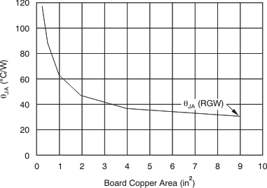
Unfortunately, this thermal resistance (θJA) is highly dependent on the heat-spreading capability built into the particular PCB design, and therefore varies according to the total copper area, copper weight, and location of the planes. The θJA recorded in the Thermal Information table is determined by the JEDEC standard, PCB, and copper-spreading area and is only used as a relative measure of package thermal performance. Note that for a well-designed thermal layout, θJA is actually the sum of the VQFN package junction-to-case (bottom) thermal resistance (θJCbot) plus the thermal resistance contribution by the PCB copper. When θJCbot is known, the amount of heat-sinking area required can be estimated for a given θJA, as shown in Figure 53. θJCbot can be found in the Thermal Information table.
8.1.5 Estimating Junction Temperature
The JEDEC standard now recommends the use of psi (Ψ) thermal metrics to estimate the junction temperatures of the LDO when in-circuit on a typical PCB board application. These metrics are not strictly speaking thermal resistances, but rather offer practical and relative means of estimating junction temperatures. These psi metrics are determined to be significantly independent of the copper-spreading area. The key thermal metrics (ΨJT and ΨJB) are given in the Thermal Information table and are used in accordance with Equation 11.

where
- PD is the power dissipated as explained in Equation 9,
- TT is the temperature at the center-top of the device package, and
- TB is the PCB surface temperature measured 1 mm from the device package and centered on the package edge.
8.2 Typical Application
This section discusses the implementation of the TPS7A8300 using the ANY-OUT configuration to regulate a 1.6-A load requiring good PSRR at high frequency with low-noise at 1.2 V using a 1.4-V input voltage. The schematic for this typical application circuit is provided in Figure 54.
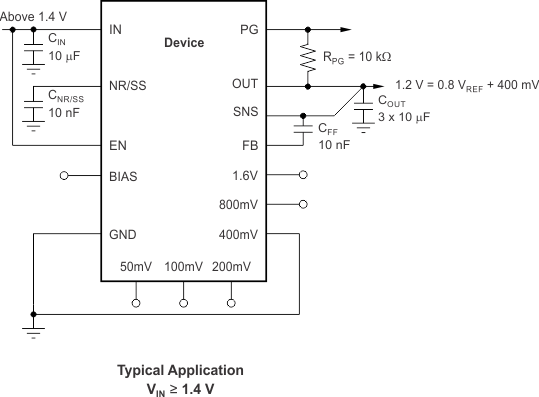 Figure 54. Typical Application
8.2.1 Design Requirements
For this design example, use the parameters listed in Table 4 as the input parameters.
Table 4. Design Parameters
| PARAMETER | DESIGN REQUIREMENT |
|---|---|
| Input voltage | 1.4 V, ±3%, provided by the dc/dc converter switching at 1 MHz |
| Output voltage | 1.2 V, ±1% |
| Output current | 1.6 A (maximum), 10 mA (minimum) |
| RMS noise, 10 Hz to 100 kHz | < 20 µVRMS |
| PSRR at 1 MHz | > 40 dB |
| Startup time | < 10 ms |
8.2.2 Detailed Design Procedure
At 1.6 A, the dropout of the TPS7A8300 has 150 mV maximum dropout over temperature, thus a 200-mV headroom is sufficient for operation over both input and output voltage accuracy. The efficiency of the TPS7A8300 in this configuration is VOUT / VIN = 85.7%.
To achieve the smallest form factor, the 3.5-mm × 3.5-mm2 RGR package is selected. The ANY-OUT internal resistor network is also used.
To achieve 1.2 V on the output, the 400mV pin is grounded. The voltage value of 400 mV is added to the 0.8-V internal reference voltage for VOUT(NOM) equal to 1.2 V; as described in Equation 12.
Input and output capacitors are selected in accordance with the Capacitor Recommendation section. Ceramic capacitances of 10 µF for the input and three 10-µF capacitors for the output are selected.
To satisfy the required startup time and still maintain low noise performance, a 10-nF CNR/SS is selected. This value is calculated with Equation 13.
With an efficiency of 85.7% and a 1.6-A maximum load, the internal power dissipation is 320 mW, which corresponds to a 11.3°C junction temperature rise for the RGR package. With an 85°C maximum ambient temperature, the junction temperature is at 96.3°C. To minimize noise, a feed-forward capacitance (CFF) of 10 nF is selected.
8.2.3 Application Curves
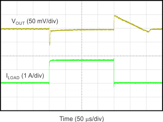 Figure 55. Output Load Transient Response
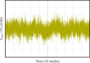 Figure 56. 10-Hz to 100-kHz Output Noise Voltage, 1.6-A Load Current
8.3 Do's and Don'ts
Do place at least one 22-µF ceramic capacitor as close as possible to the OUT terminal of the regulator.
Do not place the output capacitor more than 10 mm away from the regulator.
Do connect a 10-μF low equivalent series resistance (ESR) capacitor across the IN pin and GND input of the regulator.
Do not exceed the absolute maximum ratings.
Do not float the Enable pin.
