-
TCA9416 Ultra-Low-Voltage I2C Translator with Rise Time Accelerators
TCA9416 Ultra-Low-Voltage I2C Translator with Rise Time Accelerators
1 Features
- 2-bit bidirectional translator for SDA and SCL lines in I2C applications
- Provides bidirectional voltage translation with no direction pin
- High-impedance output SCL_A, SDA_A, SCL_B, SDA_B pins when OE = 0 V or VCC = 0 V
- Internal 10-kΩ pull-up resistor on all SDA and SCL pins are enabled based on respective VCC voltage
- 1.08 V to 3.6 V on both A and B ports
- VCC Isolation feature: If either VCC input is at GND, both ports are in the high-impedance state (excluding pull-ups)
- No power-supply sequencing required: either VCCA or VCCB can be ramped first
- Low Ioff of 2.5 µA when either VCCA or VCCB = 0 V
- OE input can be tied directly to VCCA or controlled by GPIO
- Latch-up performance exceeds 100 mA per JESD 78, class II
- ESD Protection exceeds JESD 22
- 2500-V Human-body model (A114-B)
- 1500-V Charged-device model (C101)
2 Applications
3 Description
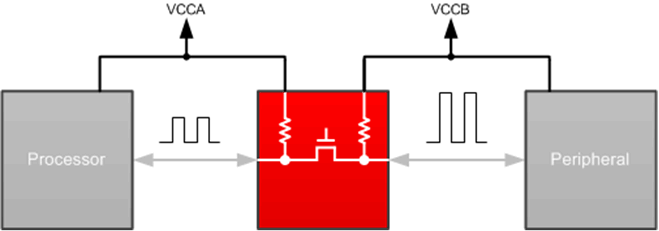
The TCA9416 is a 2-bit bidirectional I2C and SMBus voltage-level translator with an output enable (OE) input and rising and falling edge accelerators. It is operational from 1.08 V to 3.6 V on both the A-side and B-side. This allows the device to interface between lower and higher logic signal levels at any of the typical 1.2-V, 1.8-V, 2.5-V, and 3.3-V supply rails.
The OE input pin is referenced to VCCA, can be tied directly to VCCA, but it is also 3.6-V tolerant. The OE pin can also be controlled and set to a logic low to place all the SCL and SDA pins in a high-impedance state, which significantly reduces the quiescent current consumption.
Under normal I2C and SMBus configurations, the TCA9416 is compatible with standard speeds where the frequency of SCL is 100 kHz (Standard-mode), 400 kHz (Fast-mode), or 1 MHz (Fast-mode Plus).
The TCA9416 features internal 10-kΩ pull-up resistors on SCL_A, SDA_A, SCL_B, and SDA_B. Additional external pull-up resistors can be added to the bus to reduce the total pull-up resistance and speed up rising edges.
| PART NUMBER | PACKAGE(1) | BODY SIZE (NOM) |
|---|---|---|
| TCA9416 | X2SON (8) | 1.35 mm × 0.80 mm |
| SOT-23-T (8) | 2.9 mm × 1.6 mm |
 Typical
Application Block Diagram for TCA9416