-
SN65HVD1780, SN65HVD1781, and SN65HVD1782Functional Safety FIT Rate, FMD and Pin FMA SFFS055 March 2021 SN65HVD1780 , SN65HVD1781 , SN65HVD1782
-
SN65HVD1780, SN65HVD1781, and SN65HVD1782Functional Safety FIT Rate, FMD and Pin FMA
SN65HVD1780, SN65HVD1781, and SN65HVD1782Functional Safety FIT Rate, FMD and Pin FMA
Trademarks
All trademarks are the property of their respective owners.
1 Overview
This document contains information for SN65HVD1780, SN65HVD1781, and SN65HVD1782 (SOIC and PDIP package) to aid in a functional safety system design. Information provided are:
- Functional Safety Failure In Time (FIT) rates of the semiconductor component estimated by the application of industry reliability standards
- Component failure modes and their distribution (FMD) based on the primary function of the device
- Pin failure mode analysis (Pin FMA)
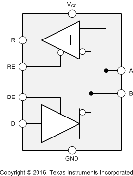
Figure 1-1 shows the device functional block diagram for reference.
 Figure 1-1 Functional Block
Diagram
Figure 1-1 Functional Block
DiagramSN65HVD1780, SN65HVD1781, and SN65HVD1782 were developed using a quality-managed development process, but were not developed in accordance with the IEC 61508 or ISO 26262 standards.
2 Functional Safety Failure In Time (FIT) Rates
This section provides Functional Safety Failure In Time (FIT) rates for SN65HVD1780, SN65HVD1781, and SN65HVD1782 based on two different industry-wide used reliability standards:
- Table 2-1 provides FIT rates based on IEC TR 62380 / ISO 26262 part 11
- Table 2-4 provides FIT rates based on the Siemens Norm SN 29500-2
| FIT IEC TR 62380 / ISO 26262 | FIT (Failures Per 109 Hours) 8-pin SOIC (D) JEDEC high-K model | FIT (Failures Per 109 Hours) 8-pin PDIP (P) JEDEC high-K model | FIT (Failures Per 109 Hours) 8-pin SOIC (D) JEDEC low-K model | FIT (Failures Per 109 Hours) 8-pin PDIP (P) JEDEC low-K model |
|---|---|---|---|---|
| Total Component FIT Rate | 19 | 27 | 13 | 23 |
| Die FIT Rate | 10 | 5 | 5 | 3 |
| Package FIT Rate | 9 | 22 | 9 | 20 |
| FIT IEC TR 62380 / ISO 26262 | FIT (Failures Per 109 Hours) 8-pin SOIC (D) JEDEC high-K model | FIT (Failures Per 109 Hours) 8-pin PDIP (P) JEDEC high-K model | FIT (Failures Per 109 Hours) 8-pin SOIC (D) JEDEC low-K model | FIT (Failures Per 109 Hours) 8-pin PDIP (P) JEDEC low-K model |
|---|---|---|---|---|
| Total Component FIT Rate | 20 | 27 | 14 | 23 |
| Die FIT Rate | 11 | 5 | 6 | 3 |
| Package FIT Rate | 9 | 22 | 8 | 20 |
| FIT IEC TR 62380 / ISO 26262 | FIT (Failures Per 109 Hours) 8-pin SOIC (D) JEDEC high-K model | FIT (Failures Per 109 Hours) 8-pin PDIP (P) JEDEC high-K model | FIT (Failures Per 109 Hours) 8-pin SOIC (D) JEDEC low-K model | FIT (Failures Per 109 Hours) 8-pin PDIP (P) JEDEC low-K model |
|---|---|---|---|---|
| Total Component FIT Rate | 26 | 30 | 16 | 25 |
| Die FIT Rate | 16 | 7 | 7 | 4 |
| Package FIT Rate | 10 | 23 | 9 | 21 |
The failure rate and mission profile information in Table 2-1 comes from the Reliability data handbook IEC TR 62380 / ISO 26262 part 11:
- Mission Profile: Motor Control from Table 11
- Power dissipation: 290 mW
- Climate type: World-wide Table 8
- Package factor (lambda 3): Table 17b
- Substrate Material: FR4
- EOS FIT rate assumed: 0 FIT
| Table | Category | Reference FIT Rate | Reference Virtual TJ |
|---|---|---|---|
| 5 | CMOS, BICMO Digital analog / mixed |
25 FIT | 55°C |
The Reference FIT Rate and Reference Virtual TJ (junction temperature) in Table 2-4 come from the Siemens Norm SN 29500-2 tables 1 through 5. Failure rates under operating conditions are calculated from the reference failure rate and virtual junction temperature using conversion information in SN 29500-2 section 4.
3 Failure Mode Distribution (FMD)
The failure mode distribution estimation for SN65HVD1780, SN65HVD1781, and SN65HVD1782 in Table 3-1 comes from the combination of common failure modes listed in standards such as IEC 61508 and ISO 26262, the ratio of sub-circuit function size and complexity and from best engineering judgment.
The failure modes listed in this section reflect random failure events and do not include failures due to misuse or overstress.
| Die Failure Modes | Failure Mode Distribution (%) |
|---|---|
| Receiver fail | 15% |
| Transmitter fail | 63% |
| I/O | 12% |
| PCU | 10% |