MSP430F2101 Microcontroller
1 Functional Advisories
Advisories that affect the device's operation, function, or parametrics.
✓ The check mark indicates that the issue is present in the specified revision.
| Errata Number | Rev L | Rev K | Rev J | Rev I | Rev H | Rev G | Rev E | Rev D | Rev C |
|---|---|---|---|---|---|---|---|---|---|
| BCL6 | ✓ | ✓ | |||||||
| BCL8 | ✓ | ✓ | |||||||
| BCL9 | ✓ | ✓ | ✓ | ✓ | |||||
| BCL10 | ✓ | ✓ | ✓ | ✓ | |||||
| BCL11 | ✓ | ✓ | ✓ | ✓ | |||||
| BCL12 | ✓ | ✓ | ✓ | ✓ | ✓ | ✓ | ✓ | ✓ | ✓ |
| BCL13 | ✓ | ✓ | ✓ | ✓ | ✓ | ||||
| BCL14 | ✓ | ✓ | ✓ | ✓ | ✓ | ||||
| CPU5 | ✓ | ||||||||
| CPU11 | ✓ | ✓ | ✓ | ✓ | ✓ | ✓ | ✓ | ✓ | ✓ |
| CPU14 | ✓ | ✓ | |||||||
| CPU45 | ✓ | ✓ | ✓ | ✓ | ✓ | ✓ | ✓ | ✓ | ✓ |
| FLASH16 | ✓ | ✓ | ✓ | ✓ | ✓ | ✓ | ✓ | ✓ | ✓ |
| FLASH17 | ✓ | ✓ | ✓ | ✓ | ✓ | ✓ | ✓ | ✓ | ✓ |
| FLASH18 | ✓ | ✓ | ✓ | ✓ | ✓ | ✓ | ✓ | ✓ | ✓ |
| FLASH19 | ✓ | ✓ | ✓ | ✓ | ✓ | ✓ | ✓ | ✓ | ✓ |
| FLASH20 | ✓ | ✓ | ✓ | ✓ | ✓ | ✓ | ✓ | ✓ | ✓ |
| FLASH22 | ✓ | ✓ | ✓ | ✓ | |||||
| FLASH24 | ✓ | ✓ | ✓ | ✓ | ✓ | ✓ | ✓ | ✓ | ✓ |
| FLASH27 | ✓ | ✓ | ✓ | ✓ | ✓ | ✓ | ✓ | ✓ | ✓ |
| FLASH36 | ✓ | ✓ | ✓ | ✓ | ✓ | ✓ | ✓ | ✓ | ✓ |
| PORT8 | ✓ | ✓ | |||||||
| PORT10 | ✓ | ✓ | ✓ | ✓ | |||||
| SYS15 | ✓ | ✓ | ✓ | ✓ | ✓ | ✓ | ✓ | ✓ | ✓ |
| TA12 | ✓ | ✓ | ✓ | ✓ | ✓ | ✓ | ✓ | ✓ | ✓ |
| TA16 | ✓ | ✓ | ✓ | ✓ | ✓ | ✓ | ✓ | ✓ | ✓ |
| TA21 | ✓ | ✓ | ✓ | ✓ | ✓ | ✓ | ✓ | ✓ | ✓ |
| TAB22 | ✓ | ✓ | ✓ | ✓ | ✓ | ✓ | ✓ | ✓ | ✓ |
| XOSC5 | ✓ | ✓ | ✓ | ✓ | ✓ | ✓ | ✓ | ✓ | ✓ |
| XOSC8 | ✓ | ✓ | ✓ | ✓ | ✓ | ✓ | ✓ |
2 Preprogrammed Software Advisories
Advisories that affect factory-programmed software.
✓ The check mark indicates that the issue is present in the specified revision.
| Errata Number | Rev L | Rev K | Rev J | Rev I | Rev H | Rev G | Rev E | Rev D | Rev C |
|---|---|---|---|---|---|---|---|---|---|
| BSL5 | ✓ |
4 Fixed by Compiler Advisories
Advisories that are resolved by compiler workaround. Refer to each advisory for the IDE and compiler versions with a workaround.
✓ The check mark indicates that the issue is present in the specified revision.
| Errata Number | Rev L | Rev K | Rev J | Rev I | Rev H | Rev G | Rev E | Rev D | Rev C |
|---|---|---|---|---|---|---|---|---|---|
| CPU4 | ✓ | ✓ | ✓ | ✓ | ✓ | ✓ | ✓ | ✓ | ✓ |
| CPU6 | ✓ | ✓ | |||||||
| CPU12 | ✓ | ✓ | ✓ | ✓ | ✓ | ✓ | ✓ | ✓ | ✓ |
| CPU13 | ✓ | ✓ | ✓ | ✓ | ✓ | ✓ | ✓ | ✓ | ✓ |
| CPU19 | ✓ | ✓ | ✓ | ✓ | ✓ | ✓ | ✓ | ✓ | ✓ |
Refer to the following MSP430 compiler documentation for more details about the CPU bugs workarounds.
TI MSP430 Compiler Tools (Code Composer Studio IDE)
- MSP430 Optimizing C/C++ Compiler: Check the --silicon_errata option
- MSP430 Assembly Language Tools
MSP430 GNU Compiler (MSP430-GCC)
- MSP430 GCC Options: Check -msilicon-errata= and -msilicon-errata-warn= options
- MSP430 GCC User's Guide
IAR Embedded Workbench
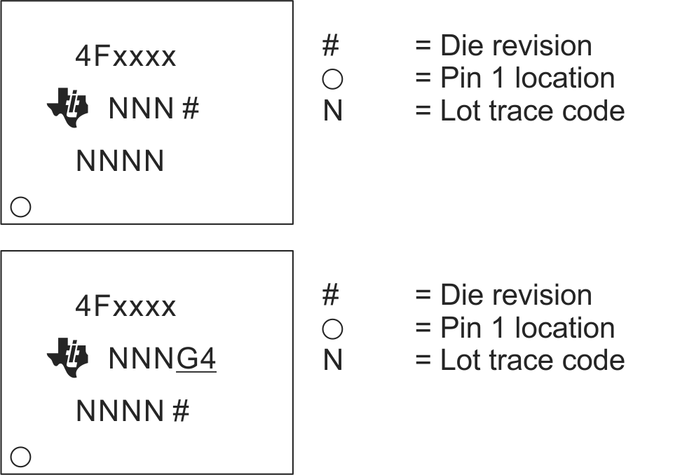
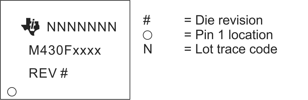
5 Nomenclature, Package Symbolization, and Revision Identification
The revision of the device can be identified by the revision letter on the Package Markings or by the HW_ID located inside the TLV structure of the device.
5.1 Device Nomenclature
To designate the stages in the product development cycle, TI assigns prefixes to the part numbers of all MSP MCU devices. Each MSP MCU commercial family member has one of two prefixes: MSP or XMS. These prefixes represent evolutionary stages of product development from engineering prototypes (XMS) through fully qualified production devices (MSP).
XMS – Experimental device that is not necessarily representative of the final device's electrical specifications
MSP – Fully qualified production device
Support tool naming prefixes:
X: Development-support product that has not yet completed Texas Instruments internal qualification testing.
null: Fully-qualified development-support product.
XMS devices and X development-support tools are shipped against the following disclaimer:
"Developmental product is intended for internal evaluation purposes."
MSP devices have been characterized fully, and the quality and reliability of the device have been demonstrated fully. TI's standard warranty applies.
Predictions show that prototype devices (XMS) have a greater failure rate than the standard production devices. TI recommends that these devices not be used in any production system because their expected end-use failure rate still is undefined. Only qualified production devices are to be used.
TI device nomenclature also includes a suffix with the device family name. This suffix indicates the temperature range, package type, and distribution format.
5.2 Package Markings
DGV20
TVSOP (DGV), 20 Pin

PW20
TSSOP (PW), 20 Pin
DW20
SOP (DW), 20 Pin
RGE24
QFN (RGE), 24 Pin

5.3 Memory-Mapped Hardware Revision (TLV Structure)
This device does not support reading the hardware revision from memory.
Further guidance on how to locate the TLV structure and read out the HW_ID can be found in the device User's Guide.
6 Advisory Descriptions
6.1 BCL6
BCL Module
Category
Functional
Function
DCO calibration error
Description
The DCO calibration values stored in the information memory may differ by up to +- 2%.
This applies to all Rev. C and the following Lot-Trace code Rev. D devices:
Lot#57FNFCK
Lot#58E081K
Lot#58E521K
Lot#58F5K9K
Lot#58F5KTK
Lot#58F860K
Lot#58F866K
Lot#58FKL3K
Lot#59C279K
Workaround
Recalibrate the DCO using a reference clock source
6.2 BCL8
BCL Module
Category
Functional
Function
Erroneous ISR DCO DC generator enable
Description
When MCLK and SMCLK are sourced from a clock other than the DCO, the SCG0 DCO control bit is erroneously cleared upon interrupt service routine entry from LPMx by the CPU. This enables the DCO DC generator causing additional current consumption. After executing the RETI instruction, the status register SCG0 bit will return to a set state turning off the DC generator, eliminating this added current. The increased current will only occur during the interrupt service routine, and is in the range of 20 uA at 3V.
Workaround
Set SCG0 in software at the beginning of an interrupt service routine. This will reduce the time that the DC generator is enabled to four MCLK.
6.3 BCL9
BCL Module
Category
Functional
Function
ACLK divider modifications require delay before entering LPM3
Description
After modifying the DIVAx bits, immediately entering LPM3 can cause the modification to be ignored and the divider settings not to take effect. Reading back the DIVAx bits will indicate the intended setting even when the divider has not been correctly applied.
Workaround
When the DIVAx bits are modified, a delay of one complete ACLK (VLO or LFXT1CLK) period must elapse before entering LPM3. The delay is only necessary the first time LPM3 is entered after the DIVAx bits are modified. After the one-period delay, LPM3 may be entered and exited normally without additional delays.
6.4 BCL10
BCL Module
Category
Functional
Function
MCLK = ACLK and P2SEL control bits
Description
When using ACLK as the CPU MCLK clock source, the oscillator failsafe feature does not automatically switch MCLK to the DCO if the P2SEL6 or P2SEL7 bit is cleared. This applies when ACLK = LFXT1 (external low frequency clock source). The CPU will halt operation since no MCLK signal is present.
Workaround
None
6.5 BCL11
BCL Module
Category
Functional
Function
Watchdog failsafe when using ACLK
Description
When using ACLK as the WDT+ clock source, the WDT+ oscillator failsafe feature does not automatically switch to the DCO if the P2SEL6 or P2SEL7 bit is cleared. This applies when ACLK = LFXT1 (external low frequency clock source). The WDT+ will halt operation since no clock signal is present.
Workaround
None
6.6 BCL12
BCL Module
Category
Functional
Function
Switching RSELx or modifying DCOCTL can cause DCO dead time or a complete DCO stop
Description
After switching RSELx bits (located in register BCSCTL1) from a value of >13 to a value of <12 OR from a value of <12 to a value of >13, the resulting clock delivered by the DCO can stop before the new clock frequency is applied. This dead time is approximately 20 us. In some instances, the DCO may completely stop, requiring a power cycle.
Furthermore, if all of the RSELx bits in the BSCTL1 register are set, modifying the DCOCTL register to change the DCOx or the MODx bits could also result in DCO dead time or DCO hang up.
Workaround
- When switching RSEL from >13 to <12, use an intermediate frequency step. The intermediate RSEL value should be 13.

AND
- When switching RSEL from <12 to >13 it's recommended to set RSEL to its default value first (RSEL = 7) before switching to the desired target frequency.
AND
- In case RSEL is at 15 (highest setting) it's recommended to set RSEL to its default value first (RSEL = 7) before accessing DCOCTL to modify the DCOx and MODx bits. After the DCOCTL register modification the RSEL bits can be manipulated in an additional step.
In the majority of cases switching directly to intermediate RSEL steps as described above will prevent the occurrence of BCL12. However, a more reliable method can be implemented by changing the RSEL bits step by step in order to guarantee safe function without any dead time of the DCO.
Note that the 3-step clock startup sequence consisting of clearing DCOCTL, loading the BCSCTL1 target value, and finally loading the DCOCTL target value as suggested in the in the "TLV Structure" chapter of the MSP430x2xx Family User's Guide is not affected by BCL12 if (and only if) it is executed after a device reset (PUC) prior to any other modifications being made to BCSCTL1 since in this case RSEL still is at its default value of 7. However any further changes to the DCOx and MODx bits will require the consideration of the workaround outlined above.
6.7 BCL13
BCL Module
Category
Functional
Function
DCO powerup halt
Description
When subject to very slow Vcc rise times, the device may enter into a state where the DCO does not oscillate. No JTAG access or program execution is possible and the device will remain in a reset state until the supply voltage is disconnected.
Workaround
Apply a Vcc poweron ramp >= 10V/second under all power-on/power-cycle scenarios.
6.8 BCL14
BCL Module
Category
Functional
Function
Oscillator fault forced in bypass mode when P2SEL.7 bit is not set
Description
When the LFXT1 oscillator is used in bypass mode and P2SEL.7 is not set, the oscillator fault flag (OFIFG) will be forced to set and cannot be cleared. Due to the failsafe logic, LFXT1 cannot be used as MCLK in this case. The bug only affects the behavior of the oscillator fault, the clocking itself works properly.
Workaround
Set both P2SEL.6 and P2SEL.7 if the application requires correct function of the oscillator fault flag (e.g. MCLK failsafe logic).
6.9 BSL5
BSL Module
Category
Software in ROM
Function
BSL might not start if RST/NMI pin is configured as NMI input
Description
If the RST/NMI pin is configured to NMI, the bootstrap loader may not be started. Unpredictable operations will result.
Workaround
None