-
LM2901-Q1, LM2901B-Q1, LM2901V-Q1, LM2901AV-Q1 Functional Safety FIT Rate, FMD and Pin FMA SLCA003 February 2023 LM2901-Q1 , LM2901AV-Q1 , LM2901B-Q1 , LM2901V-Q1
-
LM2901-Q1, LM2901B-Q1, LM2901V-Q1, LM2901AV-Q1 Functional Safety FIT Rate, FMD and Pin FMA
LM2901-Q1, LM2901B-Q1, LM2901V-Q1, LM2901AV-Q1 Functional Safety FIT Rate, FMD and Pin FMA
1 LM2901-Q1, LM2901B-Q1, LM2901V-Q1, LM2901AV-Q1 Functional Safety FIT Rate, FMD and Pin FMA
1.1 Overview
This document contains information for LM2901-Q1, LM2901B-Q1, LM2901V-Q1, LM2901AV-Q1 (TSSOP-14, SOIC-14 packages) to aid in a functional safety system design. Information provided are:
- Functional Safety Failure In Time (FIT) rates of the semiconductor component estimated by the application of industry reliability standards
- Component failure modes and their distribution (FMD) based on the primary function of the device
- Pin failure mode analysis (Pin FMA)
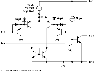
#FIGURE11 shows the device functional block diagram for reference.
 Figure 1-1 Functional Block
Diagram
Figure 1-1 Functional Block
DiagramLM2901-Q1, LM2901B-Q1, LM2901V-Q1, LM2901AV-Q1 was developed using a quality-managed development process, but was not developed in accordance with the IEC 61508 or ISO 26262 standards.
1.2 Functional Safety Failure In Time (FIT) Rates
This section provides Functional Safety Failure In Time (FIT) rates for LM2901-Q1, LM2901B-Q1, LM2901V-Q1, LM2901AV-Q1 based on two different industry-wide used reliability standards:
- Table 1-1 provides FIT rates based on IEC TR 62380 / ISO 26262 part 11
- Table 1-2 provides FIT rates based on the Siemens Norm SN 29500-2
| FIT IEC TR 62380 / ISO 26262 | FIT (Failures Per 109 Hours) | |
|---|---|---|
|
Package |
TSSOP-14 |
SOIC-14 |
| Total Component FIT Rate |
10 |
16 |
| Die FIT Rate |
2 |
2 |
| Package FIT Rate |
8 |
14 |
The failure rate and mission profile information in Table 1-1 comes from the Reliability data handbook IEC TR 62380 / ISO 26262 part 11:
- Mission Profile: Motor Control from Table 11
- Power dissipation12 mW
- Climate type: World-wide Table 8
- Package factor (lambda 3): Table 17b
- Substrate Material: FR4
- EOS FIT rate assumed: 0 FIT
| Table | Category | Reference FIT Rate | Reference Virtual TJ |
|---|---|---|---|
| 4 | CMOS, BICMOS Digital, analog / mixed |
6 FIT | 55°C |
The Reference FIT Rate and Reference Virtual TJ (junction temperature) in Table 1-2 come from the Siemens Norm SN 29500-2 tables 1 through 5. Failure rates under operating conditions are calculated from the reference failure rate and virtual junction temperature using conversion information in SN 29500-2 section 4.
1.3 Failure Mode Distribution (FMD)
The failure mode distribution estimation for LM2901-Q1, LM2901B-Q1, LM2901V-Q1, LM2901AV-Q1 in Table 1-3 comes from the combination of common failure modes listed in standards such as IEC 61508 and ISO 26262, the ratio of sub-circuit function size and complexity and from best engineering judgment.
The failure modes listed in this section reflect random failure events and do not include failures due to misuse or overstress.
| Die Failure Modes | Failure Mode Distribution (%) |
|---|---|
| Out open (HIZ) | 15% |
| Out saturate high | 25% |
| Out saturate low | 25% |
| Out functional not in specification | 30% |
| Short circuit any two pins | 5% |
1.4 Pin Failure Mode Analysis (Pin FMA)
This section provides a Failure Mode Analysis (FMA) for the pins of the LM2901-Q1, LM2901B-Q1, LM2901V-Q1, LM2901AV-Q1. The failure modes covered in this document include the typical pin-by-pin failure scenarios:
- Pin short-circuited to Ground (see Table 1-5)
- Pin open-circuited (see Table 1-6)
- Pin short-circuited to an adjacent pin (see Table 1-7)
- Pin short-circuited to supply (see Table 1-8)
Table 1-5 through Table 1-8 also indicate how these pin conditions can affect the device as per the failure effects classification in Table 1-4.
| Class | Failure Effects |
|---|---|
| A | Potential device damage that affects functionality |
| B | No device damage, but loss of functionality |
| C | No device damage, but performance degradation |
| D | No device damage, no impact to functionality or performance |
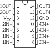
Figure 1-2 shows the LM2901-Q1, LM2901B-Q1, LM2901V-Q1, LM2901AV-Q1 pin diagram. For a detailed description of the device pins please refer to the 'Pin Configuration and Functions' section in the data sheet.
 Figure 1-2 Pin Diagram
| Pin Name | Pin No. | Description of Potential Failure Effect(s) | Failure Effect Class |
|---|---|---|---|
|
1OUT |
1 |
No change if GND pin is GND node | B |
|
2OUT |
2 |
No change if GND pin is GND node | B |
|
VCC |
3 |
Main supply shorted out (no power to device) | B |
|
2IN- |
4 |
Output goes high, if other input is positive | B |
|
2IN+ |
5 |
Output goes low, if other input is positive | B |
|
1IN- |
6 |
Output goes high, if other input is positive | B |
|
1IN+ |
7 |
Output goes low, if other input is positive | B |
|
3IN- |
8 |
Output goes high, if other input is positive | B |
|
3IN+ |
9 |
Output goes low, if other input is positive | B |
|
4IN- |
10 |
Output goes high, if other input is positive | B |
|
4IN+ |
11 |
Output goes low, if other input is positive | B |
|
GND |
12 |
No change if same node as GND | D |
|
4OUT |
13 |
No change if GND pin is GND node | B |
|
3OUT |
14 |
No change if GND pin is GND node | B |
| Pin Name | Pin No. | Description of Potential Failure Effect(s) | Failure Effect Class |
|---|---|---|---|
|
1OUT |
1 |
Output can't drive application load | B |
|
2OUT |
2 |
Output can't drive application load | B |
|
VCC |
3 |
Main supply open (no power to device) | B |
|
2IN- |
4 |
Output may be low or high | B |
|
2IN+ |
5 |
Output may be low or high | B |
|
1IN- |
6 |
Output may be low or high | B |
|
1IN+ |
7 |
Output may be low or high | B |
|
3IN- |
8 |
Output may be low or high | B |
|
3IN+ |
9 |
Output may be low or high | B |
|
4IN- |
10 |
Output may be low or high | B |
|
4IN+ |
11 |
Output may be low or high | B |
|
GND |
12 |
Lowest voltage pin will drive GND pin internally (via diode) | A |
|
4OUT |
13 |
Output can't drive application load | B |
|
3OUT |
14 |
Output can't drive application load | B |
| Pin Name | Pin No. | Shorted to | Description of Potential Failure Effect(s) | Failure Effect Class |
|---|---|---|---|---|
|
1OUT |
1 |
2OUT |
Output may be low or high | B |
|
2OUT |
2 |
VCC |
Thermal stress due to high power dissipation | A |
|
VCC |
3 |
2IN- |
Output goes low, if other input is less positive | B |
|
2IN- |
4 |
2IN+ |
Output may be low or high | B |
|
2IN+ |
5 |
1IN- |
Output may be low or high | B |
|
1IN- |
6 |
1IN+ |
Output may be low or high | B |
|
1IN+ |
7 |
3IN- |
Output may be low or high | B |
|
3IN- |
8 |
3IN+ |
Output may be low or high | B |
|
3IN+ |
9 |
4IN- |
Output may be low or high | B |
|
4IN- |
10 |
4IN+ |
Output may be low or high | B |
|
4IN+ |
11 |
GND |
Output goes low, if other input is positive | B |
|
GND |
12 |
4OUT |
No change if GND pin is GND node | B |
|
4OUT |
13 |
3OUT |
Output may be low or high | B |
|
3OUT |
14 |
1OUT |
Output may be low or high | B |
| Pin Name | Pin No. | Description of Potential Failure Effect(s) | Failure Effect Class |
|---|---|---|---|
|
1OUT |
1 |
Thermal stress due to high power dissipation | A |
|
2OUT |
2 |
Thermal stress due to high power dissipation | A |
|
VCC |
3 |
No change if same node as VCC | D |
|
2IN- |
4 |
Output goes low, if other input is less positive | B |
|
2IN+ |
5 |
Output goes high, if other input is less positive | B |
|
1IN- |
6 |
Output goes low, if other input is less positive | B |
|
1IN+ |
7 |
Output goes high, if other input is less positive | B |
|
3IN- |
8 |
Output goes low, if other input is less positive | B |
|
3IN+ |
9 |
Output goes high, if other input is less positive | B |
|
4IN- |
10 |
Output goes low, if other input is less positive | B |
|
4IN+ |
11 |
Output goes high, if other input is less positive | B |
|
GND |
12 |
Main supply shorted out (no power to device) | B |
|
4OUT |
13 |
Thermal stress due to high power dissipation | A |
|
3OUT |
14 |
Thermal stress due to high power dissipation | A |