-
TUSB320LAI, TUSB320HAI USB Type-C Configuration Channel Logic and Port Control SLLSEQ8D October 2015 – May 2017 TUSB320HAI , TUSB320LAI
PRODUCTION DATA.
-
TUSB320LAI, TUSB320HAI USB Type-C Configuration Channel Logic and Port Control
- 1 Features
- 2 Applications
- 3 Description
- 4 Revision History
- 5 Pin Configuration and Functions
- 6 Specifications
- 7 Detailed Description
- 8 Application and Implementation
- 9 Power Supply Recommendations
- 10Layout
- 11Device and Documentation Support
- 12Mechanical, Packaging, and Orderable Information
- IMPORTANT NOTICE
TUSB320LAI, TUSB320HAI USB Type-C Configuration Channel Logic and Port Control
1 Features
- USB Type-C™ Specification 1.1
- Backward Compatible with USB Type-C Specification 1.0
- Supports Up to 3 A of Current Advertisement and Detection
- Mode Configuration
- Host Only – DFP (Source)
- Device Only – UFP (Sink)
- Dual Role Port – DRP
- Supports both Try.SRC and Try.SNK
- Channel Configuration (CC)
- Attach of USB Port Detection
- Cable Orientation Detection
- Role Detection
- Type-C Current Mode (Default, Medium, High)
- VBUS Detection
- I2C or GPIO Control
- Supports up to 400 kHz I2C
- Role Configuration Control Through I2C
- Supply Voltage: 2.7 V to 5 V
- Low Current Consumption
- Industrial Temperature Range of –40 to 85°C
2 Applications
- Host, Device, Dual Role Port Applications
- Mobile Phones
- Tablets and Notebooks
- USB Peripherals
3 Description
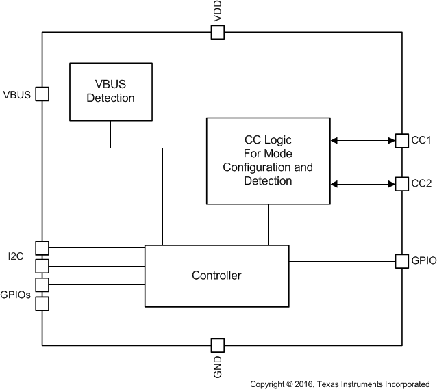
The TUSB320LA and TUSB320HA devices, hereafter called TUSB320 unless otherwise noted, are Texas Instrument's third generation Type-C configuration channel logic and port controller. The TUSB320 devices use the CC pins to determine port attach and detach, cable orientation, role detection, and port control for Type-C current mode. The TUSB320 devices can be configured as a downstream facing port (DFP), upstream facing port (UFP) or a dual role port (DRP) making them ideal for any application.
The TUSB320 devices have an alternate configuration as a DFP or UFP according to the Type-C specifications. The CC logic block monitors the CC1 and CC2 pins for pullup or pulldown resistances to determine when a USB port has been attached, the orientation of the cable, and the role detected. The CC logic detects the Type-C current mode as default, medium, or high depending on the role detected. VBUS detection is implemented to determine a successful attach in UFP and DRP modes.
The devices operate over a wide supply range and have low-power consumption. The TUSB320 is available in two versions of enable: Active low enable called TUSB320LA and active high enable called TUSB320HA. The TUSB320 family of devices are available in industrial temperature ranges.
Device Information(1)
| PART NUMBER | PACKAGE | BODY SIZE (NOM) |
|---|---|---|
| TUSB320LAI | X2QFN (12) | 1.60 mm × 1.60 mm |
| TUSB320HAI | X2QFN (12) | 1.60 mm × 1.60 mm |
- For all available packages, see the orderable addendum at the end of the data sheet.
Simplified Schematic

Sample Applications

4 Revision History
Changes from C Revision (October 2016) to D Revision
- Changed RVBUS values From: MIN = 891, TYP = 900, MAX = 909 KΩ To: MIN = 855, TYP = 887, MAX = 920 KΩ Go
Changes from B Revision (September 2016) to C Revision
- Changed text for Pin 7 in the Pin Functions table From: "default current mode detected (H); medium or high current mode detected (L)." To: "Refer to Table 3 for more details." Go
- Changed text for Pin 8 in the Pin Functions table From: "default or medium current mode detected (H); high current mode detected (L)." To: "Refer to Table 3 for more details." Go
Changes from A Revision (March 2016) to B Revision
- Changed pins CC1 and CC2 values From: MIN = –0.3 MAX = VDD + 0.3 To: MIN –0.3 MAX = 6 in the Absolute Maximum RatingsGo
Changes from * Revision (October 2015) to A Revision
- Added Note 1 and 2 to the Pin Functions tableGo
- Changed the DESCRIPTION of pin EN_N pin in the Pin Functions tableGo
- Changed the DESCRIPTION of pin EN pin in the Pin Functions tableGo
- Changed the DESCRIPTION of pin VDD in the Pin Functions tableGo
- Added Test Condition "See Figure 1" to VBUS_THR in the Electrical Characteristics Go
- Added Note 2 to the Electrical Characteristics table Go
- Changed the last sentence of the Debug Accessory sectionGo
- Added Note: "SW must make sure..." to the Description of INTERRUPT_STATUS in Table 9 Go
- Added text to list item 2 in the TUSB320LA Initialization Procedure sectionGo
- Added text to list item 2 in the TUSB320HA Initialization Procedure sectionGo
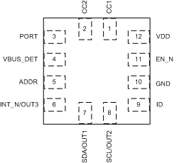
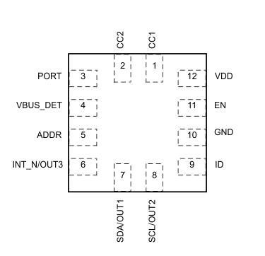
5 Pin Configuration and Functions


Pin Functions
| PIN | TYPE | DESCRIPTION | ||
|---|---|---|---|---|
| NAME | TUSB320LA | TUSB320HA | ||
| CC1 | 1 | 1 | I/O | Type-C configuration channel signal 1 |
| CC2 | 2 | 2 | I/O | Type-C configuration channel signal 2 |
| PORT(1) | 3 | 3 | I | Tri-level input pin to indicate port mode. The state of this pin is sampled when EN_N is asserted low in the TUSB320L device, EN is asserted high in the TUSB320H device, and VDD is active. This pin is also sampled following a I2C_SOFT_RESET. H - DFP (Pull-up to VDD if DFP mode is desired) NC - DRP (Leave unconnected if DRP mode is desired) L - UFP (Pull-down or tie to GND if UFP mode is desired) |
| VBUS_DET(1) | 4 | 4 | I | 5-V to 28-V VBUS input voltage. VBUS detection determines UFP attachment. One 900-kΩ external resistor required between system VBUS and VBUS_DET pin. |
| ADDR(1) | 5 | 5 | I | Tri-level input pin to indicate I2C address or GPIO mode: H — I2C is enabled and I2C 7-bit address is 0x67. NC — GPIO mode (I2C is disabled) L — I2C is enabled and I2C 7-bit address is 0x47. ADDR pin should be pulled up to VDD if high configuration is desired |
| INT_N/OUT3(1) | 6 | 6 | O | The INT_N/OUT3 is a dual-function pin. When used as the INT_N, the pin is an open drain output in I2C control mode and is an active low interrupt signal for indicating changes in I2C registers. When used as OUT3, the pin is in audio accessory detect in GPIO mode: no detection (H), audio accessory connection detected (L). |
| SDA/OUT1(1)(2) | 7 | 7 | I/O | The SDA/OUT1 is a dual-function pin. When I2C is enabled (ADDR pin is high or low), this pin is the I2C communication data signal. When in GPIO mode (ADDR pin is NC), this pin is an open drain output for communicating Type-C current mode detect when the device is in UFP mode: Refer to Table 3 for more details. |
| SCL/OUT2(1)(2) | 8 | 8 | I/O | The SCL/OUT2 is a dual function pin. When I2C is enabled (ADDR pin is high or low), this pin is the I2C communication clock signal. When in GPIO mode (ADDR pin is NC), this pin is an open drain output for communicating Type-C current mode detect when the device is in UFP mode: Refer to Table 3 for more details. |
| ID | 9 | 9 | O | Open drain output; asserted low when the CC pins detect device attachment when port is a source (DFP), or dual-role (DRP) acting as source (DFP). |
| GND | 10 | 10 | G | Ground |
| EN_N | 11 | — | I | Enable signal; active low. Pulled up to VDD internally to disable the TUSB320L device. If controlled externally, must be held low at least for 50 ms after VDD has reached its valid voltage level. |
| EN | — | 11 | I | Enable signal; active high. Pulled down to GND internally to disable the TUSB320H device. If controlled externally, must be held low at least for 50 ms after VDD has reached its valid voltage level. |
| VDD | 12 | 12 | P | Positive supply voltage. VDD must ramp within 25 ms or less |
6 Specifications
6.1 Absolute Maximum Ratings
over operating free-air temperature range (unless otherwise noted)(1)6.2 ESD Ratings
| VALUE | UNIT | |||
|---|---|---|---|---|
| V(ESD) | Electrostatic discharge | Human-body model (HBM), per ANSI/ESDA/JEDEC JS-001(1) | ±3000 | V |
| Charged-device model (CDM), per JEDEC specification JESD22-C101(2) | ±1500 | |||
6.3 Recommended Operating Conditions
over operating free-air temperature range (unless otherwise noted)| MIN | NOM | MAX | UNIT | ||
|---|---|---|---|---|---|
| VDD | Supply voltage range | 2.7 | 5 | V | |
| VBUS | System VBUS voltage | 4 | 5 | 28 | V |
| TA | TUSB320HAI and TUSB320LAI Operating free air temperature range | –40 | 25 | 85 | °C |
6.4 Thermal Information
| THERMAL METRIC(1) | TUSB320 | UNIT | |
|---|---|---|---|
| RWB (X2QFN) | |||
| 12 PINS | |||
| RθJA | Junction-to-ambient thermal resistance | 169.3 | °C/W |
| RθJC(top) | Junction-to-case (top) thermal resistance | 68.1 | °C/W |
| RθJB | Junction-to-board thermal resistance | 83.4 | °C/W |
| ψJT | Junction-to-top characterization parameter | 2.2 | °C/W |
| ψJB | Junction-to-board characterization parameter | 83.4 | °C/W |
| RθJC(bot) | Junction-to-case (bottom) thermal resistance | N/A | |
6.5 Electrical Characteristics
over operating free-air temperature range (unless otherwise noted)| PARAMETER | TEST CONDITIONS | MIN | TYP | MAX | UNIT | |
|---|---|---|---|---|---|---|
| POWER CONSUMPTION | ||||||
| IUNATTACHED_UFP | Current consumption in unattached mode when port is unconnected and waiting for connection. [VDD = 4.5 V, EN_N (TUSB320LA) = L, EN (TUSB320HA) = H, ADDR = NC, PORT = L] | 70 | µA | |||
| IACTIVE_UFP | Current consumption in active mode. [VDD = 4.5 V, EN_N (TUSB320LA) = L, EN (TUSB320HA) = H, ADDR = NC, PORT = L] | 70 | µA | |||
| ISHUTDOWN | Leakage current when VDD is supplied, but the TUSB320 device is not enabled. [VDD = 4.5 V, EN_N (TUSB320LA) = H, EN (TUSB320HA) = L] | 0.04 | µA | |||
| CC1 AND CC2 PINS | ||||||
| RCC_DB | Pulldown resistor when in dead-battery mode. | 4.1 | 5.1 | 6.1 | kΩ | |
| RCC_D | Pulldown resistor when in UFP or DRP mode. | 4.6 | 5.1 | 5.6 | kΩ | |
| VUFP_CC_USB | Voltage level range for detecting a DFP attach when configured as a UFP and DFP is advertising default current source capability. | 0.25 | 0.61 | V | ||
| VUFP_CC_MED | Voltage level range for detecting a DFP attach when configured as a UFP and DFP is advertising medium (1.5-A) current source capability. | 0.7 | 1.16 | V | ||
| VUFP_CC_HIGH | Voltage level range for detecting a DFP attach when configured as a UFP and DFP is advertising high (3-A) current source capability. | 1.31 | 2.04 | V | ||
| VTH_DFP_CC_USB | Voltage threshold for detecting a UFP attach when configured as a DFP and advertising default current source capability. | 1.51 | 1.6 | 1.64 | V | |
| VTH_DFP_CC_MED | Voltage threshold for detecting a UFP attach when configured as a DFP and advertising medium current (1.5-A) source capability. | 1.51 | 1.6 | 1.64 | V | |
| VTH_DFP_CC_HIGH | Voltage threshold for detecting a UFP attach when configured as a DFP and advertising high current (3.0-A) source capability. | 2.46 | 2.6 | 2.74 | V | |
| ICC_DEFAULT_P | Default mode pullup current source when operating in DFP or DRP mode. | 64 | 80 | 96 | µA | |
| ICC_MED_P | Medium (1.5-A) mode pullup current source when operating in DFP or DRP mode. | 166 | 180 | 194 | µA | |
| ICC_HIGH_P | High (3-A) mode pullup current source when operating in DFP or DRP mode.(1) | 304 | 330 | 356 | µA | |
| CONTROL PINS: PORT, ADDR, INT/OUT3, EN_N, EN, ID | ||||||
| VIL | Low-level control signal input voltage (PORT, ADDR, EN_N, EN) | 0.4 | V | |||
| VIM | Mid-level control signal input voltage (PORT, ADDR) | 0.28 × VDD | 0.56 × VDD | V | ||
| VIH | High-level control signal input voltage (PORT, ADDR, EN_N) | VDD – 0.3 | VDD | V | ||
| VIH_EN | High-Level control signal input voltage for EN for TUSB320HA | 1.05 | 3.65 | V | ||
| IIH | High-level input current | –20 | 20 | µA | ||
| IIL | Low-level input current | –10 | 10 | µA | ||
| IID_LEAKAGE | Current Leakage on ID pin | VDD = 0 V; ID = 5 V | 10 | µA | ||
| REN_N | Internal pullup resistance for EN_N for TUSB320LA | 1.1 | MΩ | |||
| REN | Internal pulldown resistance for EN for TUSB320HA | 500 | kΩ | |||
| Rpu(2) | Internal pullup resistance (PORT, ADDR) | 588 | kΩ | |||
| Rpd (2) | Internal pulldown resistance (PORT, ADDR) | 1.1 | MΩ | |||
| VOL | Low-level signal output voltage (open-drain) (INT_N/OUT3, ID) | IOL = –1.6 mA | 0.4 | V | ||
| Rp_ODext | External pullup resistor on open drain IOs (INT_N/OUT3, ID) | 200 | kΩ | |||
| Rp_TLext | Tri-level input external pullup resistor (PORT, ADDR) | 4.7 | kΩ | |||
| I2C - SDA/OUT1, SCL/OUT2 CAN OPERATE FROM 1.8 V OR 3.3 V (±10%)(3) | ||||||
| VDD_I2C | Supply range for I2C (SDA/OUT1, SCL/OUT2) | 1.65 | 1.8 | 3.6 | V | |
| VIH | High-level signal voltage | 1.05 | 3.6 | V | ||
| VIL | Low-level signal voltage | 0.4 | V | |||
| VOL | Low-level signal output voltage (open drain) | IOL = –1.6 mA | 0.4 | V | ||
| VBUS_DET IO PINS (CONNECTED TO SYSTEM VBUS SIGNAL) | ||||||
| VBUS_THR | VBUS threshold range | See Figure 1 | 2.95 | 3.3 | 3.8 | V |
| RVBUS | External resistor between VBUS and VBUS_DET pin | 855 | 887 | 920 | KΩ | |
| RVBUS_PD | Internal pulldown resistance for VBUS_DET | 95 | KΩ | |||
6.6 Timing Requirements
| MIN | NOM | MAX | UNIT | ||
|---|---|---|---|---|---|
| I2C (SDA, SCL) | |||||
| tSU:DAT | Data setup time | 100 | ns | ||
| tHD;DAT | Data hold time | 10 | ns | ||
| tSU:STA | Set-up time, SCL to start condition | 0.6 | µs | ||
| tHD:STA | Hold time (repeated), start condition to SCL | 0.6 | µs | ||
| tSU:STO | Set up time for stop condition | 0.6 | µs | ||
| tBUF | Bus free time between a stop and start condition | 1.3 | µs | ||
| tVD;DAT | Data valid time | 0.9 | µs | ||
| tVD;ACK | Data valid acknowledge time | 0.9 | µs | ||
| fSCL | SCL clock frequency; I2C mode for local I2C control | 400 | kHz | ||
| tr | Rise time of both SDA and SCL signals | 300 | ns | ||
| tf | Fall time of both SDA and SCL signals | 300 | ns | ||
| CBUS_100KHZ | Total capacitive load for each bus line when operating at ≤ 100 kHz | 400 | pF | ||
| CBUS_400KHz | Total capacitive load for each bus line when operating at 400 kHz | 100 | pF | ||
6.7 Switching Characteristics
over operating free-air temperature range (unless otherwise noted)| PARAMETER | TEST CONDITIONS | MIN | TYP | MAX | UNIT | |
|---|---|---|---|---|---|---|
| tCCCB_DEFAULT | Power on default of CC1 and CC2 voltage debounce time | DEBOUCE register = 2'b00 |
168 | ms | ||
| tVBUS_DB | Debounce of VBUS_DET pin after valid VBUS_THR | 2 | ms | |||
| tDRP_DUTY_CYCLE | Power-on default of percentage of time DRP advertises DFP during a tDRP | DRP_DUTY_CYCLE register = 2'b00 |
30% | |||
| tDRP | The period during which the TUSB320HA or the TUSB320LA in DFP mode completes a DFP to UFP and back advertisement. | 50 | 75 | 100 | ms | |
| tI2C_EN | Time from TUSB320LA EN_N low or TUSB320HA EN high and VDD active to I2C access available | 100 | ms | |||
| tSOFT_RESET | Soft reset duration | 26 | 49 | 95 | ms | |
 Figure 1. VBUS Detect and Debounce