Battery-Less NFC/RFID Temperature Sensing Patch
Battery-Less NFC/RFID Temperature Sensing Patch
NFC/RFID enables communication with transponders. The transponders include memory that can store various information including URLs, Bluetooth® connection handover, contact information, diagnostics, and now sensor measurement data. Battery-less sensor measurements that utilize energy harvesting from the RF field can be implemented in applications ranging from medical, health and fitness, and industrial where instantaneous measurements are required and a battery is not feasible or desired. This application report discusses the implementation of a single chip NFC/RFID field powered temperature sensor system with the RF430FRL152H.
Project collateral discussed in this application report can be downloaded from www.ti.com/lit/zip/sloc322.
Trademarks
Bluetooth is a registered trademark of Bluetooth SIG, Inc.
All other trademarks are the property of their respective owners.
1 Reference Design Hardware
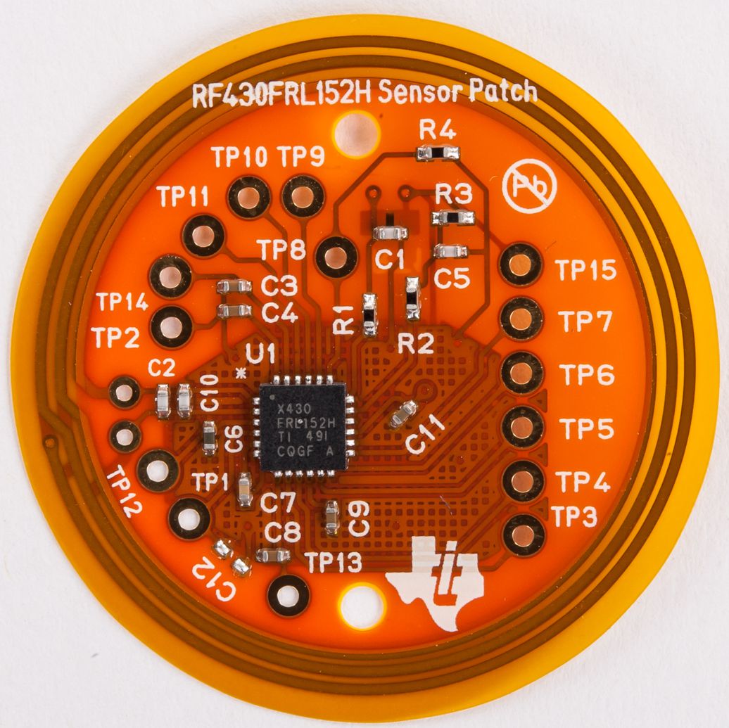
The schematic and layout are shown in Figure 1 and Figure 2. The design keeps a low component count by using integrated features of the RF430FRL152H such as the internal A/D converter and ROM functions for acquiring sensor measurements from a thermistor (RT1). This design also offers the flexibility to include a 1.5 V battery at TP1/TP2 if data logging is required and the RF field will not always be available to provide power. The hatched ground pour is used for improved RF performance.


2 Firmware Implementation
One benefit of this design is that firmware does not need to be programmed into the device. This design utilizes the ROM functions inside of the RF430FRL152H. The device is initialized “over the air” by a NFC/RFID Reader/Writer device that writes the configuration registers. Subsequently, the thermistor measurements are read out by this same Reader/Writer device. When utilizing the graphical user interface (GUI) software as discussed in Section 3, the RF430FRL152H will be configured as shown below. It is important to note that with this specific configuration, each sample requires 128 ms for acquisition. The reference resistor and thermistor must be sampled for each measurement, which brings the total conversion time to 256 ms. This is just one implementation of the ADC configuration register that can be modified to meet the needs of a given application.
- Sensor Control Register
The Sensor Control Register is used to select the thermistor to be sampled. The reference resistor (R3) is also sampled and used for Calibration.- Reference/ADC1 Sensor enabled
- Thermistor/ADC2 Sensor enabled
- Thermistor enabled, number of passes = 1
- Reference/ADC1 Sensor Configuration Register
This register is used to configure the ADC1 for the reference resistor. The configuration below sets the ADC for 10-bit resolution and requires 128 ms for each sample. In this application example, 10-bit resolution was used for this for faster conversions.- Gain = 2
- Filter Type = CIC Filter
- Oversampling = 128
- Thermistor/ADC2 Sensor Configuration Register
This register is used to configure the ADC1 for the Thermistor. The configuration below sets the ADC for 10-bit accuracy and requires 128 ms for each sample. In this application example, 10-bit resolution was used for this for faster conversions.- Gain = 2
- Filter Type = CIC Filter
- Oversampling = 128
NOTE
The configuration of the device can also be read out using the RF430FRL152H GUI “Read All Tabs” button and viewing the tabs that contain the affected registers.
3 Demonstration With TRF7970AEVM
The demonstration board can be exercised with the use of the TRF7970AEVM and the RF430FRL152H GUI. The software and complete details are available in the RF430FRL152HEVM User's Guide (SLAU607).
Step-by-step instructions for use with this specific reference design are listed below:
- Install the RF430FRL152H GUI and drivers as shown in the Installation of the Software and Drivers section of the RF430FRL152HEVM User's Guide (SLAU607).
- Plug in the TRF7970AEVM, open the RF430FRL152H GUI, and click “Connect to TRF7970AEVM” (as shown in Figure 3).
- Select the “RF430FRL152H Patch” and then click the “Demo Mode” tab (as shown in Figure 4).
- Align the Patch Board in parallel with the TRF7970AEVM antenna and then click “Start Demo” (as shown in Figure 5. First, this writes the configuration for the ADC and frequency of measurements to the RF430FRL152H. Then, it begins reading the subsequent sensor measurements as they are updated.
- As long as the patch board stays within range of the TRF7970AEVM antenna, the measurements will continue to be taken and plotted on the graph (as shown in Figure 6). The latest measurement is shown as a numeric value, 78.8°F, in Figure 6. The GUI also provides the option to display in Fahrenheit or Celsius.
 Figure 3. Connect to TRF7970AEVM
  Figure 4. Select RF430FRL152H Patch
  Figure 5. Start Demo
  Figure 6. Temperature Measurements