-
Phase-Shifted Full-Bridge Converter Fundamentals
Phase-Shifted Full-Bridge Converter Fundamentals
Abstract
The phase-shifted full-bridge converter (PSFB) is common in high-performance power supplies with fast transient response, high power density and high converter efficiency. This topic reviews PSFB operation principles, characteristics of the PSFB, different types of rectifiers, clamp options, converter control modes, synchronous rectifier operation modes and light-load management options. A PSFB design based on the Modular Hardware-System-Common Redundant Power Supply (M-CRPS) base specification demonstrates the ability of a PSFB – with an active clamp circuit – to achieve a high-power design with a high transient response.
1 Introduction
Today’s power-conversion systems demand high efficiency, high power density and lighter weight. In telecommunication, server and PC applications, the 80 Plus certification program has defined efficient power-supply standards for over 15 years. Recently, the Open Compute Project (OCP) announced the M-CRPS specification for server power-supply units (PSUs), which requires even higher efficiency requirements than 80 Plus, as shown in Table 1.
| Efficiency at | 10% load | 20% load | 50% load | 100% load | Note |
|---|---|---|---|---|---|
| 80 Plus Titanium | 90% | 94% | 96% | 91% | @230-VAC input |
| M-CRPS (<2,500 W) | 90% | 94% | 96% | 92% | @240-VAC input |
| M-CRPS (≥2,500 W) | 90% | 94% | 96% | 94% | @240-VAC input |
Part of the reason why a PSU needs to have higher efficiency is because of the need for energy-efficient data centers. In data centers less than a decade old, the power usage effectiveness (PUE) is about 3, where PUE is defined in Equation 1 as:
The lower the PUE, the more efficient the data center.
Figure 1 and Figure 2 break down the power consumption of two data centers with a PUE equal to 3 and 1.25, respectively. For the data center with the PUE equal to 3, because a large portion of total data center power is powering the cooling system, increasing server PSU efficiency will definitely help reduce the cooling power needed, reducing the PUE and increasing efficiency.
 Figure 1 Data center (PUE = 3) power
consumption breakdown.
 Figure 2 Data center (PUE = 1.25) power
consumption breakdown.
Figure 2 Data center (PUE = 1.25) power
consumption breakdown.Not only is higher efficiency mandatory, but server PSUs must deliver more power in a smaller footprint given the emergence of artificial intelligence (AI) and edge computing, along with the continuation of Moore’s law. Server loads including the CPU and graphics processing unit (GPU) require much more power, as the transistors per process unit are increasing exponentially. While server rack size remains the same, server PSUs must have higher power density to meet server load power demands.
High power density is also a requirement for automotive and aerospace applications, as lighter weight means that transportation carriers will have better energy efficiency.
Inside the PSU, one way to reduce weight is to increase the converter switching frequency, which then reduces the magnetic volt-seconds and therefore its size. Figure 3 plots transformer volume versus switching frequency. An onboard charger with a DC/DC converter switching frequency of 500 kHz will have a transformer with less than half the volume of a 100-kHz transformer.
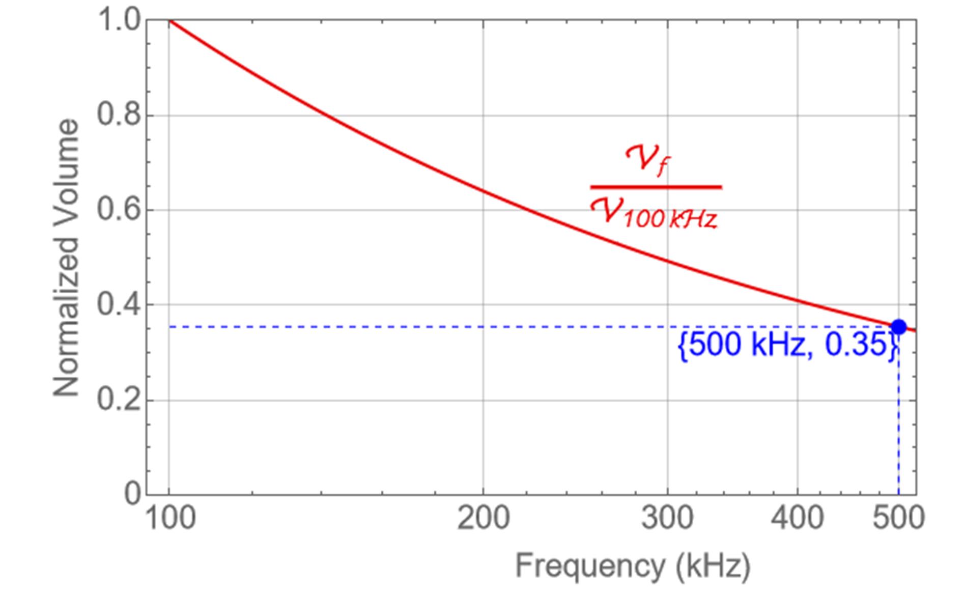 Figure 3 Transformer volume vs. switching
frequency.
Figure 3 Transformer volume vs. switching
frequency.Because the goal is to have higher power density without compromising efficiency, it is essential to introduce soft switching in the PSU to reduce switching losses. Hard-switched converters were first developed in switch-mode power supplies, which have metal-oxide semiconductor field-effect transistor (MOSFET) current and voltage overlapping at the MOSFET turnon transient, as shown in Figure 4. A higher switching frequency means more frequent hard-switching transients, and therefore more switching losses. Although it is possible to reduce switching losses by increasing the turnon speed to reduce the overlapped area, a higher voltage-changing slew rate will result in higher noise and electromagnetic interference levels. On the other hand, allowing the negative drain-to-source current to discharge the MOSFET output capacitor (Coss) voltage before the gate voltage goes high does achieve soft-switched turnon, as shown in Figure 5. The lack of current and voltage overlap at the MOSFET turnon transient results in no turnon switching losses, which allows the PSU to operate at a high switching frequency and maintain high efficiency at the same time.
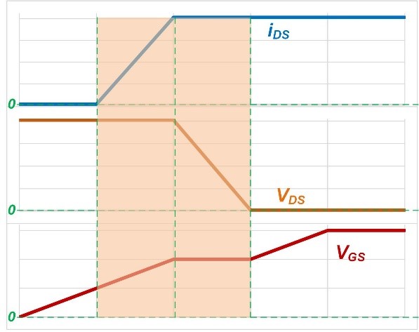 Figure 4 MOSFET hard-switching turnon
transient.
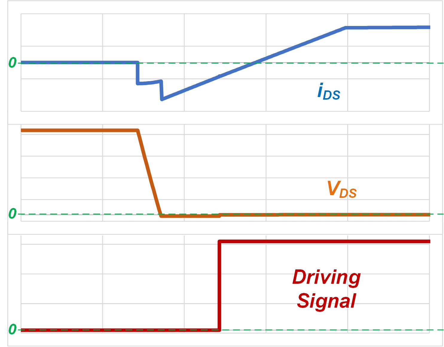 Figure 5 MOSFET soft-switching turnon
transient.
Figure 5 MOSFET soft-switching turnon
transient.The same topology with a different control method could result in different behaviors at MOSFET switching transients. Take the full-bridge converter in Figure 6 as an example. If you were to operate the full-bridge converter with pulse-width modulation (PWM) control, the converter would exhibit hard switching behavior at the MOSFET turnon transient; the MOSFET drain-to-source current starts from positive at the turnon transient.
Figure 7 shows the most significant hard-switched full-bridge converter MOSFET voltage and current waveforms, where nonzero voltage and current overlap at the switching transient, as highlighted by the green dashed-line circle. When operating the full-bridge converter with phase-shift control between the two input legs, a negative drain-to-source current during the MOSFET turnon transient will avoid nonzero voltage current overlapping for soft switching, as shown in Figure 8.
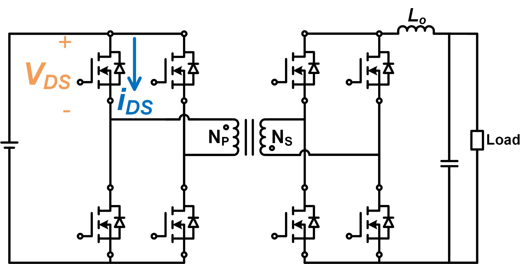 Figure 6 Full-bridge converter.
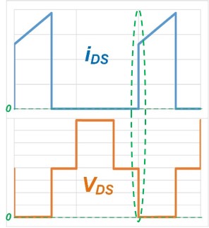 Figure 7 Hard-switched full-bridge MOSFET
current and voltage.
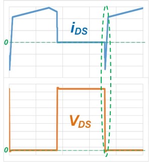 Figure 8 PSFB MOSFET current and
voltage.
Figure 8 PSFB MOSFET current and
voltage.A PFSB converter, inductor-inductor-capacitor (LLC) series resonant converter (SRC) and dual active bridge (DAB) converter can all achieve soft switching, but with different characteristics. An LLC-SRC uses frequency modulation for voltage regulation, while a PSFB and DAB both use phase-shift control with a fixed switching frequency for voltage regulation. An LLC-SRC is the only converter among these three that can achieve soft switching on the output rectifier; it usually has higher peak efficiency than the PSFB or DAB in most cases.
An LLC-SRC isn’t a good option for applications with wide input or output ranges, however. For an LLC-SRC to cover wide input or output ranges, you will have to decrease the ratio of the transformer magnetizing inductance to the resonant inductance, which will result in an efficiency reduction. A PSFB and DAB can cover wide input or output ranges with a wide effective duty-cycle (Deff) range without as much of an efficiency reduction penalty as an LLC-SRC. Moreover, peak current-mode control for a PSFB is more mature than current-mode control in an LLC-SRC for fast response to load transients. A PSFB is also the preferred choice in applications with fast transient response requirements. PSFB applications include server PSUs for AI and edge computing with fast load transients as well as battery charger applications, including electric vehicle 400-V, 800-V to 12-V battery power-conversion systems with wide input and output ranges.
In this topic, we will describe the fundamentals of a PSFB including operational principles, rectifier options, clamping options and different types of controls, along with a design example.
2 PSFB Operational Principles
Figure 9 shows a full-bridge converter with a diode rectifier, while Figure 10 shows full-bridge converter waveforms under phase-shifted control, which allows a negative drain-to-source current before the MOSFET turns on transients for soft switching. As shown in Figure 10, a phase difference is created between leg 1 MOSFET driving signals (Out1L and Out1H) and leg 2 MOSFET driving signals (Out2L and Out2H), while all four driving signals keep their duty cycle unchanged. When a diagonal pair of MOSFETs turn on, either the input voltage (+VIN) or inversed input voltage (–VIN) is applied to VAB, which is the time between the energizing of the series inductor (LS) and the delivery of energy from the input side (the primary side) to the output side (the secondary side) through the transformer. The phase difference between leg 1 and leg 2 determines the nonzero voltage duration (pulse width) of VAB. A bipolar square wave similar to the VAB waveform is generated at the secondary voltage (VSEC), which will be further rectified by the output diode rectifier to become a unipolar square wave, thus allowing the output inductor to perform “buck” operation for output regulation controlled by the VSEC pulse width.
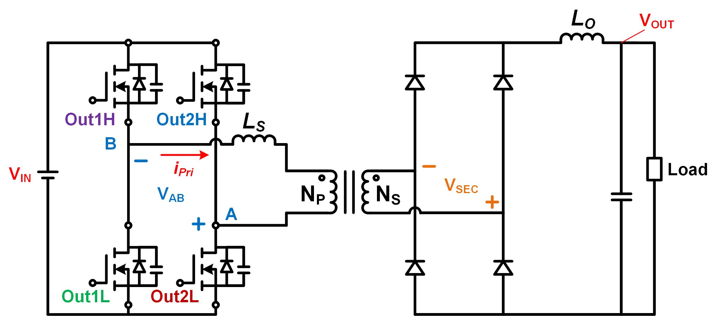 Figure 9 A PSFB with a full-bridge
rectifier.
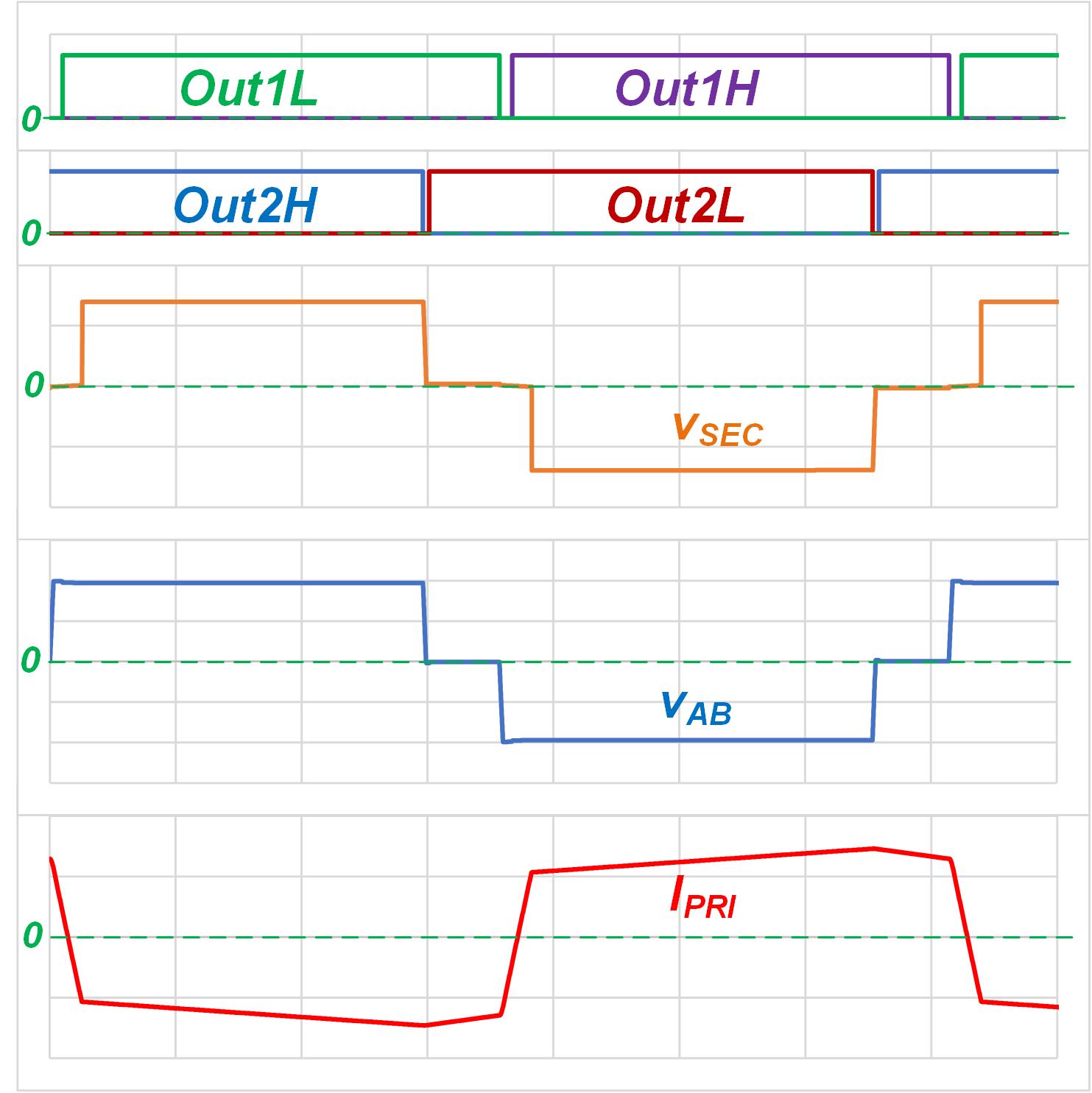 Figure 10 PSFB waveforms.
The pulse width of VSEC is smaller than VAB because LS uses the applied VIN to switch its current polarity, resulting in zero voltage on the transformer winding and thus a smaller VSEC pulse width, which is known as the duty-cycle loss. The larger the LS inductance, the larger the duty-cycle loss (the difference of pulse widths between VAB and VSEC). Enabling a larger Deff on the secondary side for a wider duty-cycle variation range requires the use of a smaller LS inductance.
Energy stored in LS during switching transients is the key to realizing soft switching at the primary-side MOSFETs. A small LS inductance means less energy stored, which could be insufficient to discharge the MOSFET output capacitor voltage for soft switching, especially at light loads. Thus, you must make a trade-off between soft switching and the Deff ranges in your design.
Because phase-shifted control enables the primary winding current to continuously circulate and freely flow through the primary full-bridge MOSFETs’ Coss and body diodes, there may be current lagging on the MOSFETs with inductive impedance at the output of the full-bridge switch nodes and negative current at the MOSFET switching transients, as shown previously in Figure 8. Energy stored in LS is the key to soft switching, but output inductor LO also affects soft-switching capability.
Let’s look at the waveform of MOSFET switching transients. The dashed purple curve in Figure 11 is the leg 1 high-side MOSFET current. Notice that the leg 1 low-side MOSFET current is identical to the leg 1 high-side MOSFET current but happens at the leg 1 high-side MOSFET turnoff period. You can see that the primary current (IPRI) level at the MOSFET turnon transient is at the LO current ripple valley point. In other words, leg 1 MOSFET’s soft-switching capability will drop if the LO current ripple is large (that is, if the LO inductance is smaller). Assuming that the transformer magnetizing inductor current is zero, Equation 2 expresses the current used to achieve soft switching at the leg 1 MOSFETs as:
where ILO,pp is the peak-to-peak current ripple on LO.
Equation 3 calculates the current used to achieve soft switching at leg 2 MOSFETs as:
Figure 12 highlights the leg 2 low-side MOSFET current with a dashed black line. Notice that the leg 2 high-side MOSFET current is identical to the leg 2 low-side MOSFET current, but happens at the leg 2 low-side MOSFET turnoff period. From Equation 2 and Equation 3, as well as the waveforms in Figure 11 and Figure 12, you can see that it is easier to achieve soft switching for MOSFETs on leg 2 than on leg 1.
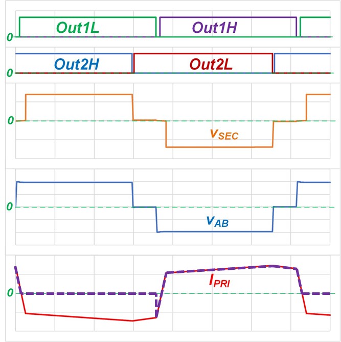 Figure 11 PSFB waveforms highlighting
leg 1 high-side MOSFET current with a dashed purple line.
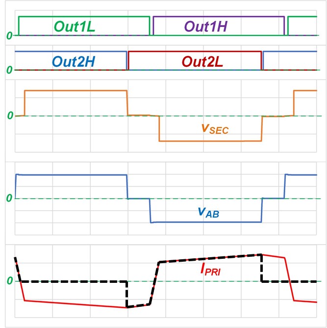 Figure 12 PSFB waveforms highlighting
leg 2 low-side MOSFET current with a dashed black line.
Figure 12 PSFB waveforms highlighting
leg 2 low-side MOSFET current with a dashed black line.3 PSFB Output Rectifiers
The primary function of the rectifier stage in a PSFB is to rectify the bipolar square wave from the transformer winding to a unipolar square wave at the input side of LO. The type of rectifier that you choose will vary based on different applications and requirements. Figure 13 through Figure 15 illustrate three popular rectifiers – the full-bridge rectifier, center-tapped rectifier and current-doubler rectifier – while Figure 16 and Figure 17 show rectifier-related waveforms.
With a full-bridge rectifier, a diagonal pair of diodes conducts current to energize LO when the transformer secondary winding voltage is positive, and the other diagonal pair of diodes conducts current to energize LO when the transformer secondary winding voltage is negative.
With a center-tapped rectifier, one output diode conducts current to energize LO when the transformer secondary winding voltage is positive; the other output diode conducts current to energize LO when the transformer secondary winding voltage is negative.
With a current-doubler rectifier, LO1 is only energized through one diode when the transformer secondary winding voltage is positive, and LO2 is only energized through the other diode when the transformer secondary winding voltage is negative.
Table 2 lists the differences among these rectifiers. For a PSFB with both full-bridge and center-tapped rectifiers, the LO operating frequency is double the primary-side MOSFET’s switching frequency because of bipolar-to-unipolar waveform conversion. The output inductors of the PSFB with a current-doubler rectifier operate at the same frequency as the primary-side MOSFET’s switching frequency. The current-doubler rectifier structure also means that the maximum Deff on the output inductors can only be 50%, while it can be 100% with full-bridge or center-tapped rectifiers.
It is also notable that each rectifier diode has a voltage stress of 2 VOUT/Deff for center-tapped rectifiers and a voltage stress of VOUT/Deff for full-bridge and current-doubler rectifiers. A full-bridge rectifier will have lower rectifier voltage stress compared to a center-tapped rectifier with the same Deff and output voltage (VOUT). Since the maximum Deff of a current-doubler rectifier can only go up to 50%, current-doubler and center-tapped rectifiers will both have higher voltage stress levels than a full-bridge rectifier in efficiency-optimized designs (with Deff closed to its maximum) with the same VOUT.
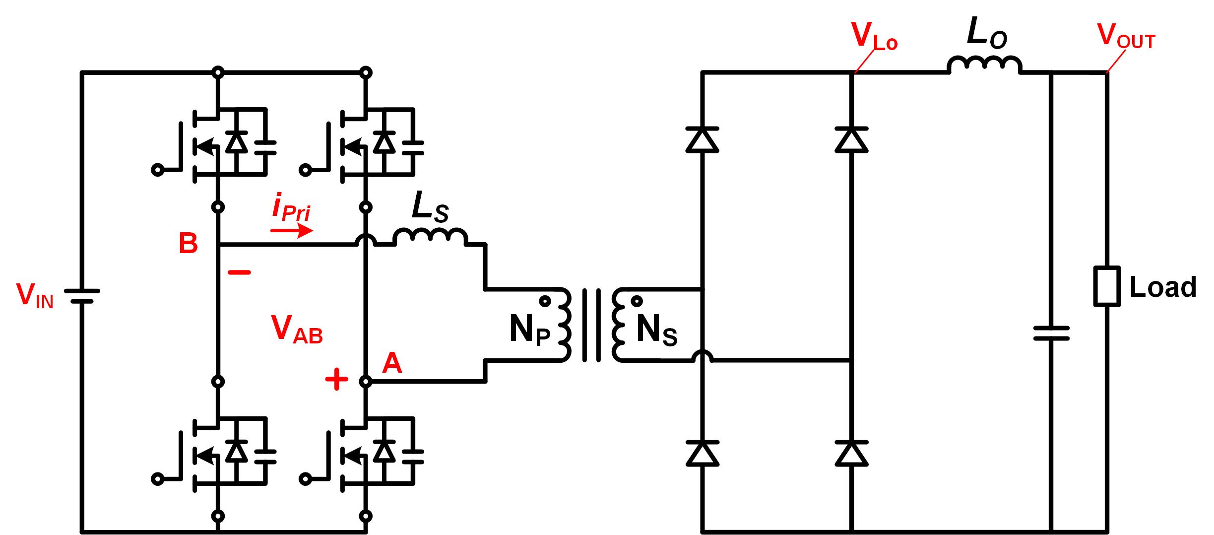 Figure 13 A PSFB with a full-bridge
rectifier.
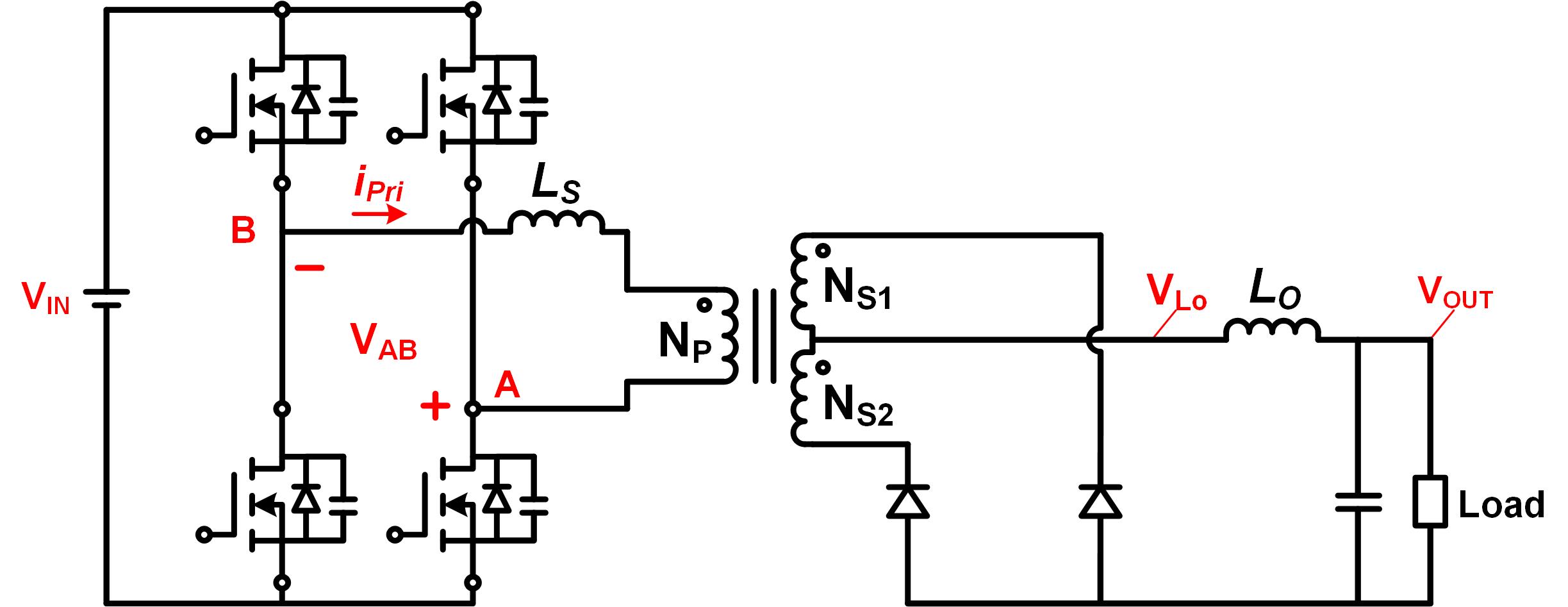 Figure 14 A PSFB with a center-tapped
rectifier.
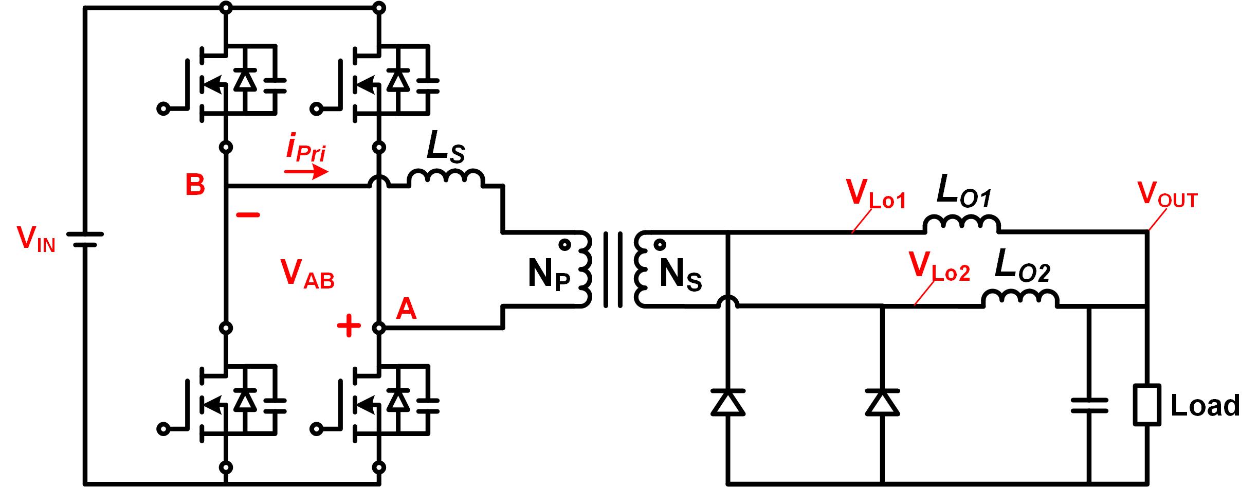 Figure 15 A PSFB with a current-doubler
rectifier.
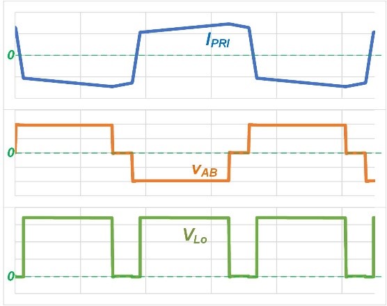 Figure 16 Waveforms of a PSFB.
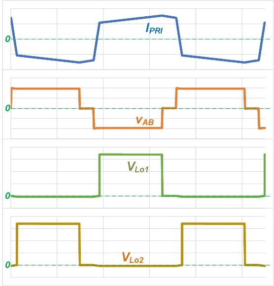 Figure 17 Waveforms of a PSFB with
either a full-bridge rectifier or a center-tapped rectifier.
| Rectifier type | Inductor operating frequency | Allowed Deff range | Number of secondary windings | Number of rectifier components | Number of output inductors | Characteristics |
|---|---|---|---|---|---|---|
| Full bridge | Twice the primary switching frequency | 0-100% | 1 | 4 | 1 | Better transformer utilization rate, good for high quiescent output voltage (Vo) |
| Center tapped | Twice the primary switching frequency | 0-100% | 2 | 2 | 1 | Lowest component count, lower transformer utilization rate |
| Current doubler | The primary switching frequency | 0-50% | 1 | 2 | 2 | Better transformer utilization rate, half ILO |