-
bq2408x 750-mA Single-Chip Li-Ion and Li-Pol Charge Management IC With Thermal Regulation
- 1 Features
- 2 Applications
- 3 Description
- 4 Revision History
- 5 Device Options
- 6 Pin Configuration and Functions
- 7 Specifications
-
8 Detailed Description
- 8.1 Overview
- 8.2 Functional Block Diagram
- 8.3
Feature Description
- 8.3.1 Control Logic Overview
- 8.3.2 Temperature Qualification (Applies Only to Versions With TS Pin Option)
- 8.3.3 Input Overvoltage Detection, Power Good Status Output
- 8.3.4 Charge Status Outputs
- 8.3.5 Battery Charging: Constant Current Phase
- 8.3.6 Charge Current Translator
- 8.3.7 Battery Voltage Regulation
- 8.3.8 Pre-Charge Timer
- 8.3.9 Thermal Protection Loop
- 8.3.10 Thermal Shutdown And Protection
- 8.3.11 Dynamic Timer Function
- 8.3.12 Charge Termination Detection and Recharge
- 8.3.13 Battery Absent Detection - Voltage Mode Algorithm
- 8.3.14 Charge Safety Timer
- 8.3.15 Short-Circuit Protection
- 8.3.16 Startup With Deeply Depleted Battery Connected
- 8.4 Device Functional Modes
- 9 Application and Implementation
- 10Power Supply Recommendations
- 11Layout
- 12Device and Documentation Support
- 13Mechanical, Packaging, and Orderable Information
- IMPORTANT NOTICE
bq2408x 750-mA Single-Chip Li-Ion and Li-Pol Charge Management IC With Thermal Regulation
1 Features
- Ideal for Low-Dropout Designs for Single-Cell Li-Ion or Li-Pol Packs in Space Limited Applications
- Integrated Power FET and Current Sensor for up to 750-mA Charge Applications
- Reverse Leakage Protection Prevents Battery Drainage
- ±0.5% Voltage Regulation Accuracy
- Thermal Regulation Maximizes Charge Rate
- Charge Termination by Minimum Current and Time
- Precharge Conditioning With Safety Timer
- Status Outputs for LED or System Interface Indicate Charge, Fault, and Power Good Outputs
- Short-Circuit and Thermal Protection
- Automatic Sleep Mode for Low Power Consumption
- Small 3×3 mm MLP Package
- Selectable Battery Insertion and Battery Absent Detection
- Input Overvoltage Protection
2 Applications
- PDA, MP3 Players, Digital Cameras
- Internet Appliances and Handheld Devices
3 Description
The bq2408x series are highly integrated Li-Ion and Li-Pol linear chargers, targeted at space-limited portable applications. The bq2408x series offers a variety of protection features and functional options, while still implementing a complete charging system in a small package. The battery is charged in three phases: conditioning, constant or thermally regulated current, and constant voltage. Charge is terminated based on minimum current. An internal programmable charge timer provides a backup protection feature for charge termination and is dynamically adjusted during the thermal regulation phase. The bq2408x automatically restarts the charge if the battery voltage falls below an internal threshold; sleep mode is set when the external input supply is removed. Multiple versions of this device family enable easy design of the bq2408x in cradle chargers or in the end equipment, while using low cost or high-end AC adapters.
Device Information(1)
| PART NUMBER | PACKAGE | BODY SIZE (NOM) |
|---|---|---|
| bq2408x | VSON (10) | 3.00 mm × 3.00 mm |
- For all available packages, see the orderable addendum at the end of the data sheet.
4 Revision History
Changes from D Revision (August 2009) to E Revision
- Added ESD Ratings table, Feature Description section, Device Functional Modes, Application and Implementation section, Power Supply Recommendations section, Layout section, Device and Documentation Support section, and Mechanical, Packaging, and Orderable Information sectionGo
5 Device Options
| CHARGE VOLTAGE | INPUT OVERVOLTAGE | TERMINATION ENABLE | SAFETY TIMER ENABLE | POWER GOOD STATUS | IC ENABLE | PACK TEMP | PACK VOLTAGE DETECTION (ABSENT) | DEVICES(1)(2) |
|---|---|---|---|---|---|---|---|---|
| 4.2 V | 6.5 V | TMR pin | TMR pin | PG pin | No | TS pin | With timer enabled | bq24086DRCR |
| bq24086DRCT | ||||||||
| 4.2 V | 6.5 V | TMR pin | TMR pin | PG pin | CE pin | No | With timer enabled | bq24085DRCR |
| bq24085DRCT | ||||||||
| 4.2 V | 6.5 V | TE pin | TMR pin | No | CE pin | No | With termination enabled | bq24087DRCR |
| bq24087DRCT | ||||||||
| 4.2 V | 10.5 V | TMR pin | TMR pin | PG pin | No | TS pin | With timer enabled | bq24088DRCR |
| bq24088DRCT |
6 Pin Configuration and Functions

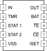
Pin Functions
| PIN | I/O | DESCRIPTION | |||
|---|---|---|---|---|---|
| NAME | bq24086/8 | bq24085 | bq24087 | ||
| BAT | 9 | 9 | 9 | I | Battery voltage sense input. Connect to the battery positive terminal. Connect a 390-Ω resistor from BAT to OUT for I(OUT) < 200 mA. |
| CE | – | 8 | 7 | I | Charge enable input. CE = LO enables charger. CE = HI disables charger. |
| IN | 1 | 1 | 1 | I | Charge input voltage and internal supply. Connect a 1-μF (minimum) capacitor from IN to VSS. CIN ≥ COUT |
| ISET | 6 | 6 | 6 | O | Charge current set point, resistor connected from ISET to VSS sets charge current value. Connect a 0.1-μF capacitor from BAT to ISET for I(OUT) < 200 mA. |
| OUT | 10 | 10 | 10 | O | Charge current output. Connect to the battery positive terminal. Connect a 1-μF (minimum) capacitor from OUT to VSS. |
| PG | 7 | 7 | O | Power good status output (open-collector), active low. | |
| STAT1 | 3 | 3 | 3 | O | Charge status output 1 (open-collector, see Table 3). |
| STAT2 | 4 | 4 | 4 | O | Charge status output 2 (open-collector, see Table 3). |
| TE | – | – | 8 | I | Termination enable input. TE = LO enables termination detection and battery absent detection. TE = HI disables termination detection and battery absent detection. |
| TMR | 2 | 2 | 2 | I | Safety timer program input, timer disabled if floating. Connect a resistor to VSS pin to program safety timer timeout value. |
| TS | 8 | – | – | I | Temperature sense input, connect to battery pack thermistor. Connect an external resistive divider to program temperature thresholds. |
| VSS | 5 | 5 | 5 | I | Ground |
| Exposed Thermal Pad | Pad | Pad | Pad | – | There is an internal electrical connection between the exposed thermal pad and Vss pin of the IC. The exposed thermal pad must be connected to the same potential as the VSS pin on the printed circuit board. Do not use the thermal pad as the primary ground input for the IC. VSS pin must be connected to ground at all times. |
7 Specifications
7.1 Absolute Maximum Ratings(1)
| MIN | MAX | UNIT | ||
|---|---|---|---|---|
| Supply voltage (IN with respect to Vss) | –0.3 | 20 | V(2) | |
| Input voltage on IN, STATx, PG, TS, CE, TMR (all with respect to Vss) | –0.3 | V(IN) | V | |
| Input voltage on OUT, BAT, ISET (all with respect to Vss) | –0.3 | 7 | V | |
| Output sink current (STATx) + PG | 15 | mA | ||
| Output current (OUT pin) | 2 | A | ||
| TA | Operating free-air temperature | –40 | 155 | °C |
| TJ | Junction temperature | –40 | 150 | °C |
| Tstg | Storage temperature | –65 | 150 | °C |
7.2 ESD Ratings
| VALUE | UNIT | |||
|---|---|---|---|---|
| V(ESD) | Electrostatic discharge | Human-body model (HBM), per ANSI/ESDA/JEDEC JS-001(1) | ±3000 | V |
| Charged-device model (CDM), per JEDEC specification JESD22-C101(2) | ±1500 | |||
7.3 Recommended Operating Conditions
| MIN | MAX | UNIT | |||
|---|---|---|---|---|---|
| V(IN) | Supply voltage | Battery absent detection not functional | 3.5 | 4.35 | V |
| V(IN) | Supply voltage | Battery absent detection functional | 4.35 | 6.5 | V |
| R(TMR) | Safety timer program resistor | 33 | 100 | KΩ | |
| TJ | Junction temperature | 0 | 125 | °C | |
7.4 Thermal Information
| THERMAL METRIC(1) | bq2408x | UNIT | |
|---|---|---|---|
| DRC (VSON) | |||
| 10 PINS | |||
| RθJA | Junction-to-ambient thermal resistance | 46.7 | °C/W |
| RθJC(top) | Junction-to-case (top) thermal resistance | 65.9 | °C/W |
| RθJB | Junction-to-board thermal resistance | 21.3 | °C/W |
| ψJT | Junction-to-top characterization parameter | 1.6 | °C/W |
| ψJB | Junction-to-board characterization parameter | 21.4 | °C/W |
| RθJC(bot) | Junction-to-case (bottom) thermal resistance | 3.6 | °C/W |
7.5 Electrical Characteristics
over recommended operating range, TJ = 0 –125°C range, See the Application and Implementation section, typical values at TJ = 25°C (unless otherwise noted), RTMR = 49.9 KΩ| PARAMETER | TEST CONDITIONS | MIN | TYP | MAX | UNIT | ||
|---|---|---|---|---|---|---|---|
| POWER DOWN THRESHOLD – UNDERVOLTAGE LOCKOUT | |||||||
| VUVLO | Power down threshold | V(IN) = 0 V, increase V(OUT): 0 → 3 V OR V(OUT) = 0 V, increase V(IN): 0 → 3 V, CE = LO (1) |
1.5 | 3 | V | ||
| INPUT POWER DETECTION(2) | |||||||
| VIN(DT) | Input power detection threshold | V(IN) detected at [V(IN) – V(OUT)] > VIN(DT) | 130 | mV | |||
| VHYS(INDT) | Input power detection hysteresis | Input power not detected at [V(IN) – V(OUT)] < [VIN(DT) – VHYS(INDT)] |
30 | mV | |||
| INPUT OVERVOLTAGE PROTECTION | |||||||
| V(OVP) | Input overvoltage detection threshold | V(IN) increasing | bq24088 | 10.2 | 10.5 | 11.7 | V |
| bq24085/6/7 | 6.2 | 6.5 | 7 | ||||
| VHYS(OVP) | Input overvoltage hysteresis | V(IN) decreasing | bq24088 | 0.5 | V | ||
| bq24085/6/7 | 0.2 | ||||||
| QUIESCENT CURRENT | |||||||
| ICC(CHGOFF) | IN pin quiescent current, charger off | Input power detected, CE = HI |
V(IN) = 6 V | 100 | 200 | μA | |
| V(IN) = 16.5 V | 350 | ||||||
| ICC(CHGON) | IN pin quiescent current, charger on | Input power detected, CE = LO, VBAT = 4.5 V | 4 | 6 | mA | ||
| IBAT(DONE) | Battery leakage current after termination into IC | Input power detected, charge terminated, CE = LO |
1 | 5 | μA | ||
| IBAT(CHGOFF) | Battery leakage current into IC, charger off | Input power detected, CE = HI OR
input power not detected, CE = LO |
1 | 5 | μA | ||
| TS PIN COMPARATOR | |||||||
| V(TS1) | Lower voltage temperature threshold | Hot detected at V(TS) < V(TS1); NTC thermistor | 29 | 30 | 31 | %V(IN) | |
| V(TS2) | Upper voltage temperature threshold | Cold detected at V(TS) > V(TS2); NTC thermistor | 60 | 61 | 62 | %V(IN) | |
| VHYS(TS) | Hysteresis | Temp OK at V(TS) > [ V(TS1) + VHYS(TS) ] OR V(TS) < [ V(TS2) – VHYS(TS) ] |
2 | %V(IN) | |||
| CE INPUT | |||||||
| VIL | Input (low) voltage | V(/CE) | 0 | 1 | V | ||
| VIH | Input (high) voltage | V(/CE) | 2 | V | |||
| STAT1, STAT2 AND PG OUTPUTS(3) | |||||||
| VOL | Output (low) saturation voltage | Iout = 1 mA (sink) | 200 | mV | |||
| THERMAL SHUTDOWN | |||||||
| T(SHUT) | Temperature trip | Junction temperature, temp rising | 155 | °C | |||
| T(SHUTHYS) | Thermal hysteresis | Junction temperature | 20 | °C | |||
| VOLTAGE REGULATION(4) | |||||||
| VO(REG) | Output voltage | 4.20 | V | ||||
| VO(TOL) | Voltage regulation accuracy | TA = 25°C | –0.5% | 0.5% | |||
| –1% | 1% | ||||||
| V(DO) | Dropout voltage, V(IN) – V(OUT) | I(OUT) = 750 mA | 600 | mV | |||
| CURRENT REGULATION(5) | |||||||
| IO(OUT) | Output current range | V(BAT) > V(LOWV), IO(OUT) = I(OUT) = K(SET) × V(SET)/R(SET) | 50 | 750 | mA | ||
| V(SET) | Output current set voltage | V(ISET) = V(SET), V(LOWV) < V(BAT) ≤ VO(REG) | 2.45 | 2.5 | 2.55 | V | |
| K(SET) | Output current set factor | 100 mA ≤ IO(OUT) ≤ 750 mA | 175 | 182 | 190 | ||
| 10 mA ≤ IO(OUT) < 100 mA | 180 | 215 | 250 | ||||
| RISET | External resistor range | Resistor connected to ISET pin | 0.6 | 10 | kΩ | ||
| PRECHARGE AND OUTPUT SHORT-CIRCUIT CURRENT REGULATION(6) | |||||||
| V(LOWV) | Precharge to fast-charge transition threshold | V(BAT) increasing | 2.8 | 2.95 | 3.15 | V | |
| V(SC) | Precharge to short-circuit transition threshold | V(BAT) decreasing | 1.2 | 1.4 | 1.6 | V | |
| V(SCIND) | Short-circuit indication | V(BAT) decreasing | 1.6 | 1.8 | 2 | ||
| IO(PRECHG) | Precharge current range | V(SC) < VI(BAT) < V(LOWV), t < t(PRECHG)
IO(PRECHG) = K(SET) × V(PRECHG)/R(ISET) |
5 | 75 | mA | ||
| V(PRECHG) | Precharge set voltage | V(ISET) = V(PRECHG), V(SC) < VI(BAT) < V(LOWV), t < t(PRECHG) |
225 | 250 | 280 | mV | |
| IO(SHORT) | Output shorted regulation current | VSS ≤ V(BAT) ≤ V(SCI), IO(SHORT) = I(OUT), V(BAT)= VSS, Internal pullup resistor, TJ = 25°C |
VPOR < VIN < 6.0 V | 7 | 15 | 24 | mA |
| 6.0 V < VIN < VOVP | 15 | ||||||
| TEMPERATURE REGULATION (Thermal regulation™)(7) | |||||||
| TJ(REG) | Temperature regulation limit | V(IN) = 5.5 V, V(BAT) = 3.2 V, Fast charge current set to 1 A | 101 | 112 | 125 | °C | |
| I(MIN_TJ(REG)) | Minimum current in thermal regulation | V(LOWV) < V(BAT) < VO(REG), 0.7 kΩ < R(ISET) < 1.18 kΩ |
105 | 125 | mA | ||
| CHARGE TERMINATION DETECTION(9) | |||||||
| I(TERM) | Termination detection current range | V(BAT) > V(RCH), I(TERM) = K(SET) × V(TERM)/R(ISET) | 5 | 75 | mA | ||
| V(TERM) | Charge termination detection set voltage(8) | V(BAT) > V(RCH) | 225 | 250 | 275 | mV | |
| BATTERY RECHARGE THRESHOLD | |||||||
| V(RCH) | Recharge threshold detection | [VO(REG)–V(BAT) ] > V(RCH) | 75 | 100 | 135 | mV | |
| TIMERS(10) | |||||||
| VTMR(OFF) | Charge timer and termination enable threshold | Charge timer AND termination disabled at: V(TMR) > VTMR(OFF) | bq24085/86/88 | 2.5 | 3 | 3.5 | V |
| Charge timer enable threshold | Charge timer disabled at: V(TMR) > VTMR(OFF) |
bq24087 | |||||
| BATTERY DETECTION THRESHOLDS | |||||||
| IDET(DOWN) | Battery detection current (sink) | 2 V < V(BAT) < VO(REG) | 1 | 2 | 3.2 | mA | |
| IDET(UP) | Battery detection current (source) | 2 V < V(BAT) < VO(REG) | IO(PRECHG) | mA | |||
| TIMER FAULT RECOVERY | |||||||
| I(FAULT) | Fault Current (source) | V(OUT) < V(RCH) | 0.8 | 1.1 | mA | ||
| OUTPUT CURRENT SAFETY LIMIT(11) | |||||||
| I(SETSC) | Charge overcurrent safety | V(ISET) = VSS | 1.5 | A | |||
7.6 Timing Requirements
over recommended operating range, TJ = 0 –125°C range, See the Application and Implementation section, typical values at TJ = 25°C (unless otherwise noted), RTMR = 49.9 KΩ| PARAMETER | TEST CONDITIONS | MIN | TYP | MAX | UNIT | ||
|---|---|---|---|---|---|---|---|
| POWER DOWN THRESHOLD – UNDERVOLTAGE LOCKOUT | |||||||
| tDGL(PG) | Deglitch time on power good | V(IN) = 0 V → 5 V in 1 μs to PG:HI → LO |
2 | ms | |||
| INPUT POWER DETECTION(1) | |||||||
| tDGL(NOIN) | Delay time, input power not detected status(2) | PG: LO →HI after tDGL(NOIN) | 10 | μs | |||
| tDLY(CHGOFF) | Charger off delay | Charger turned off after tDLY(CHGOFF), Measured from PG: LO → HI; Timer reset after tDLY(CHGOFF) | 25 | ms | |||
| INPUT OVERVOLTAGE PROTECTION | |||||||
| tDGL(OVDET) | Input overvoltage detection delay | CE = HI or LO, Measured from V(IN) > V(OVP) to PG: LO → HI; VIN increasing |
100 | μs | |||
| tDGL(OVNDET) | Input overvoltage not detected delay(2) | CE = HI or LO, Measured from V(IN) < V(OVP)
to PG: HI → LO; V(IN) decreasing |
100 | μs | |||
| VOLTAGE AND CURRENT REGULATION TIMING(3) | |||||||
| tPWRUP(CHG) | Input power detection to full charge current time delay | Measured from PG:HI → LO to I(OUT) > 100 mA, CE = LO, IO(OUT) = 750 mA, V(BAT) = 3.5 V |
25 | ms | |||
| tPWRUP(EN) | Charge enable to full charge current delay | Measured from CE:HI → LO to I(OUT) >100 mA, IO(OUT) = 750 mA, V(BAT)= 3.5 V, V(IN) = 4.5 V, Input power detected | 25 | ms | |||
| tPWRUP(LDO) | Input power detection to voltage regulation delay, LDO mode set, no battery or load connected | Measured from PG:HI → LO to V(OUT) > 90% of charge voltage regulation; V(TMR) = OPEN, LDO mode set, no battery and no load at OUT pin, CE = LO |
25 | ms | |||
| CHARGE TERMINATION DETECTION(4) | |||||||
| tDGL(TERM) | Deglitch time, termination detected | V(ISET) decreasing | 50 | ms | |||
| BATTERY RECHARGE THRESHOLD | |||||||
| tDGL(RCH) | Deglitch time, recharge detection | V(BAT) decreasing | 350 | ms | |||
| TIMERS(5) | |||||||
| t(CHG) | Charge safety timer range | t(CHG) = K(CHG) × RTMR ; thermal loop not active | 3 | 10 | hours | ||
| K(CHG) | Charge safety timer constant | V(BAT) > V(LOWV) | 0.08 | 0.1 | 0.12 | hr/kΩ | |
| t(PCHG) | Pre-charge safety timer range | t(PCHG) = K(PCHG) × t(CHG) ; Thermal regulation loop not active | 1080 | 3600 | s | ||
| K(PCHG) | Pre-charge safety timer constant | V(BAT) < V(LOWV) | 0.08 | 0.1 | 0.12 | ||
| BATTERY DETECTION THRESHOLDS | |||||||
| t(DETECT) | Battery detection time | 2 V < V(BAT) < VO(REG), Thermal regulation loop not active; RTMR = 50 kΩ, IDET(down) or IDET (UP) | 125 | ms | |||
7.7 Dissipation Ratings(1)
| PACKAGE | θJC (°C/W) | θJA (°C/W) |
|---|---|---|
| 10-pin DRC | 3.21 | 46.87 |
7.8 Typical Characteristics
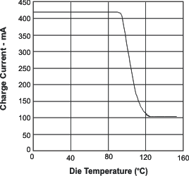
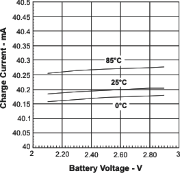
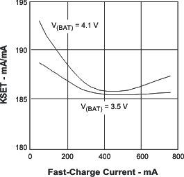
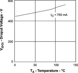
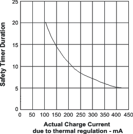
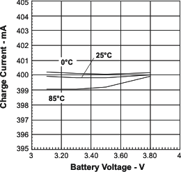
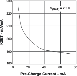
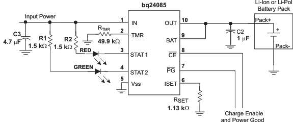
Measured using the typical application circuit shown previously.