SLUSBD1B MARCH 2013 – September 2016 BQ24715
PRODUCTION DATA.
- 1 Features
- 2 Applications
- 3 Description
- 4 Pin Configuration and Function
- 5 Specifications
-
6 Detailed Description
- 6.1 Overview
- 6.2 Functional Block Diagram
- 6.3
Feature Description
- 6.3.1 Switching Frequency Adjust
- 6.3.2 High Accuracy Current Sense Amplifiers
- 6.3.3 Charger Timeout
- 6.3.4 Input Over-Current Protection (ACOC)
- 6.3.5 Converter Over-Current Protection
- 6.3.6 Battery Over-Voltage Protection (BATOVP)
- 6.3.7 System Over-Voltage Protection (SYSOVP)
- 6.3.8 Thermal Shutdown Protection (TSHUT)
- 6.3.9 Adapter Over-Voltage Protection (ACOVP)
- 6.3.10 Adapter Detect and ACOK Output
- 6.3.11 ACFET/RBFET Control
- 6.3.12 DPM
- 6.3.13 Buck Converter Power up
- 6.4 Device Functional Modes
- 6.5 Programming
- 7 Application and Implementation
- 8 Power Supply Recommendations
- 9 Layout
- 10Device and Documentation Support
- 11Mechanical, Packaging, and Orderable Information
1 Features
- 6-24V Input SMBus NVDC-1 2-3S Battery Charger Controller
- System Instant-on Operation with No Battery or Deeply Discharged Battery
- Ultra-Fast Transient Response of 100 µs
- Ultra-Low Quiescent Current of 500 µA and High PFM Light Load Efficiency 80% at 20mA load to Meet Energy Star and ErP Lot6
- Switching Frequency: 600kHz/800kHz/1MHz
- Programmable System/Charge Voltage (16 mV/step), Input/Charge Current (64 mA/step) with High Accuracy
- ±0.5% Charge Voltage Regulation
- ±3% Input/Charge Current Regulation
- ±2% 40x Input/16x Discharge Current Monitor Output
- Support Battery LEARN Function
- Maximize CPU Performance with Deeply Discharged Battery or No Battery
- Integrated NMOS ACFET and RBFET Driver
- 20-pin 3.5 x 3.5 mm2 QFN Package
2 Applications
- Ultrabook, Notebook, and Tablet PC
- Industrial and Medical Equipment
- Portable Equipment
3 Description
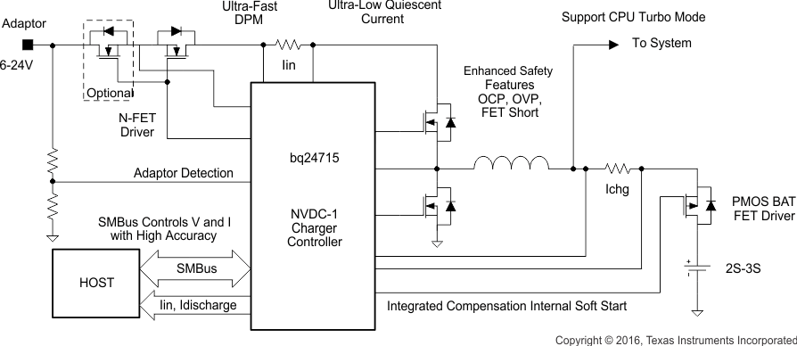
The bq24715 is a NVDC-1 synchronous battery charge controller with low quiescent current, high light load efficiency for 2S or 3S Li-ion battery charging applications, offering low component count.
The power path management allows the system to be regulated at battery voltage but does not drop below the programmable system minimum voltage.
The bq24715 provides N-channel ACFET and RBFET drivers for the power path management. It also provides driver of the external P-channel battery FET. The loop compensation is fully integrated.
The bq24715 has programmable 11-bit charge voltage, 7-bit input/charge current and 6-bit minimal system voltage with very high regulation accuracies through the SMBus communication interface.
The v monitors adapter current or battery discharge current through the IOUT pin allowing the host to throttle down CPU speed when needed.
The bq24715 provides extensive safety features for over current, over voltage and MOSFET short circuit.
Device Information(1)
| PART NUMBER | PACKAGE | BODY SIZE (NOM) |
|---|---|---|
| bq24715 | VQFN (20) | 3.50 mm × 3.50 mm |
- For all available packages, see the orderable addendum at the end of the datasheet.
Simplified Application Diagram
