-
UCC21520-Q1 4A, 6A, 5.7kVRMS Isolated Dual-Channel Gate Driver for Automotive
- 1
- 1 Features
- 2 Applications
- 3 Description
- 4 Pin Configuration and Functions
-
5 Specifications
- 5.1 Absolute Maximum Ratings
- 5.2 ESD Ratings (Automotive)
- 5.3 Recommended Operating Conditions
- 5.4 Thermal Information
- 5.5 Power Ratings
- 5.6 Insulation Specifications
- 5.7 Safety Limiting Values
- 5.8 Electrical Characteristics
- 5.9 Timing Requirements
- 5.10 Switching Characteristics
- 5.11 Insulation Characteristics Curves
- 5.12 Typical Characteristics
- 6 Parameter Measurement Information
- 7 Detailed Description
-
8 Application and Implementation
- 8.1 Application Information
- 8.2
Typical Application
- 8.2.1 Design Requirements
- 8.2.2
Detailed Design Procedure
- 8.2.2.1 Designing INA/INB Input Filter
- 8.2.2.2 Select External Bootstrap Diode and its Series Resistor
- 8.2.2.3 Gate Driver Output Resistor
- 8.2.2.4 Gate to Source Resistor Selection
- 8.2.2.5 Estimate Gate Driver Power Loss
- 8.2.2.6 Estimating Junction Temperature
- 8.2.2.7 Selecting VCCI, VDDA/B Capacitor
- 8.2.2.8 Dead Time Setting Guidelines
- 8.2.2.9 Application Circuits with Output Stage Negative Bias
- 8.2.3 Application Curves
- 9 Power Supply Recommendations
- 10Layout
- 11Device and Documentation Support
- 12Revision History
- 13Mechanical, Packaging, and Orderable Information
- IMPORTANT NOTICE
UCC21520-Q1 4A, 6A, 5.7kVRMS Isolated Dual-Channel Gate Driver for Automotive
1 Features
- Qualified for automotive applications
- AEC-Q100 qualified with the following results:
- Device temperature grade 1
- Functional safety quality-managed
- Junction temperature range –40 to +150°C
- Switching parameters:
- 33ns typical propagation delay
- 20ns minimum pulse width
- 6ns maximum pulse-width distortion
- Common-mode transient immunity (CMTI) greater than 125V/ns
- Surge immunity up to 10kV
- Isolation barrier life >40 years
- 4A peak source, 6A peak sink output
- 3V to 18V input VCCI range to interface with both digital and analog controllers
- Up to 25V VDD output drive supply
- 5V and 8V VDD UVLO options
- Programmable overlap and dead time
- Fast disable for power sequencing
- Safety-related certifications:
- 8000VPK reinforced Isolation per DIN EN IEC 60747-17 (VDE 0884-17)
- 5.7kVRMS isolation for 1 minute per UL 1577
- CSA certification per IEC 60950-1, IEC 62368-1, IEC 61010-1 and IEC 60601-1 end equipment standards
- CQC certification per GB4943.1-2022
2 Applications
- HEV and BEV battery chargers
- Isolated converters in DC-DC and AC-DC power supplies
- Uninterruptible power supply (UPS)
3 Description
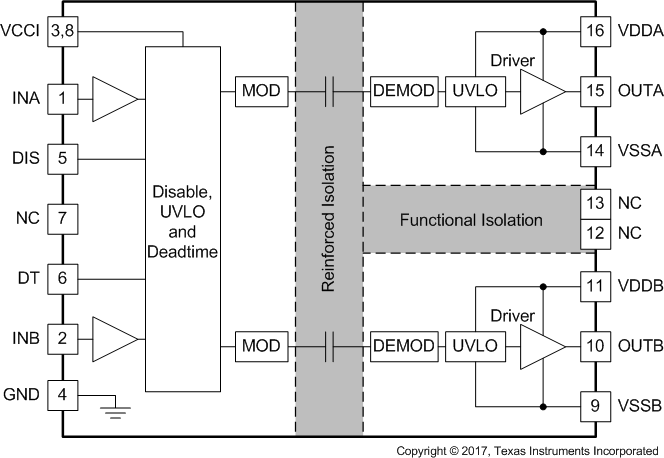
The UCC21520-Q1 is an isolated dual-channel gate driver with 4A source and 6A sink peak current. It is designed to drive power MOSFETs, IGBTs, and SiC MOSFETs up to 5MHz.
The input side is isolated from the two output drivers by a 5.7kVRMS reinforced isolation barrier, with a minimum of 125V/ns common-mode transient immunity (CMTI). Internal functional isolation between the two secondary-side drivers allows a working voltage of up to 1500VDC.
Every driver can be configured as two low-side drivers, two high-side drivers, or a half-bridge driver with programmable dead time (DT). A disable pin shuts down both outputs simultaneously , and allows normal operation when left open or grounded. As a fail-safe measure, primary-side logic failures force both outputs low.
Each device accepts VDD supply voltages up to 25V. A wide input VCCI range from 3V to 18V makes the driver suitable for interfacing with both analog and digital controllers. All supply voltage pins have under voltage lock-out (UVLO) protection.
With all these advanced features, the UCC21520-Q1 enables high efficiency, high power density, and robustness.
| PART NUMBER | PACKAGE(1) | UVLO Level |
|---|---|---|
| UCC21520-Q1 | DW (SOIC 16) | 8 V |
| UCC21520A-Q1 | DW (SOIC 16) | 5 V |
 Functional Block Diagram