-
BQ25601DI2C Controlled 3-A Single-Cell Battery Charger With USB Charger Detection for High Input Voltage and Narrow Voltage DC (NVDC) Power Path Management
- 1 Features
- 2 Applications
- 3 Description
- 4 Revision History
- 5 Description (continued)
- 6 Device Comparison Table
- 7 Pin Configuration and Functions
- 8 Specifications
-
9 Detailed Description
- 9.1 Overview
- 9.2 Functional Block Diagram
- 9.3 Feature Description
- 9.4 Device Functional Modes
- 9.5 Protections
- 9.6 Programming
- 9.7
Register Maps
- 9.7.1 REG00 (address = 00) [reset = 00010111]
- 9.7.2 REG01 (address = 01) [reset = 00011010]
- 9.7.3 REG02 (address = 02) [reset = 10100 010]
- 9.7.4 REG03 (address = 03) [reset = 001 0001 0]
- 9.7.5 REG04 (address = 04) [reset = 01011000]
- 9.7.6 REG05 (address = 05) [reset = 10011111]
- 9.7.7 REG06 (address = 06) [reset = 01100110]
- 9.7.8 REG07 (address = 07) [reset = 01001100]
- 9.7.9 REG08 (address = 08) [reset = xxxxxxxx]
- 9.7.10 REG09 (address = 09) [reset = xxxxxxxx]
- 9.7.11 REG0A (address = 0A) [reset = xxxxxx00]
- 9.7.12 REG0B (address = 0B) [reset = 00111xxx]
- 10Layout
- 11Device and Documentation Support
- IMPORTANT NOTICE
DATA SHEET
BQ25601DI2C Controlled 3-A Single-Cell Battery Charger With USB Charger Detection for High Input Voltage and Narrow Voltage DC (NVDC) Power Path Management
1 Features
- High-efficiency, 1.5-MHz, synchronous switch-mode buck charger
- 92% Charge efficiency at 2 A from 5-V input
- Optimized for USB voltage input (5 V)
- Selectable low power Pulse Frequency Modulation (PFM) Mode for light load operations
- Supports USB On-The-Go (OTG)
- Boost converter with up to 1.2-A output
- 92% Boost efficiency at 1-A output
- Accurate Constant Current (CC) limit
- Soft-start up to 500-µF capacitive load
- Output short circuit protection
- Selectable low power PFM Mode for light load operations
- Single input to support USB input and high voltage adapters
- Support 3.9-V to 13.5-V input voltage range with 22-V absolute maximum input voltage rating
- Programmable input current limit (100 mA to 3.2 a with 100-mA Resolution) to support USB 2.0, USB 3.0 standards and high voltage adaptors (IINDPM)
- Maximum power tracking by input voltage limit up to 5.4 V (VINDPM)
- VINDPM Threshold automatically tracks battery voltage
- Auto detect USB BC1.2, SDP, CDP, DCP and non-standard adaptors
- High battery discharge efficiency with 19.5-mΩ battery discharge MOSFET
- Narrow VDC (NVDC) power path management
- Instant-on works with no battery or deeply discharged battery
- Ideal diode operation in Battery Supplement Mode
- BATFET Control to support ship mode, wake up and full system reset
- Flexible autonomous and I2C Mode for optimal system performance
- High integration includes all MOSFETs, current sensing and loop compensation
- 17-µA Low battery leakage current
- High accuracy
- ±0.5% Charge voltage regulation
- ±5% at 1.5-A Charge current regulation
- ±10% at 0.9-A Input current regulation
- Safety-Related
Certifications:
- TUV IEC 62368 Certification
2 Applications
- Smart phones
- Portable internet devices and accessory
3 Description
The BQ25601D device is a highly-integrated 3-A switch-mode battery charge management and system power path management device for single cell Li-Ion and Li-polymer battery. The low impedance power path optimizes switch-mode operation efficiency, reduces battery charging time and extends battery life during discharging phase. The I2C serial interface with charging and system settings makes the device a truly flexible solution.
Device Information(1)
| PART NUMBER | PACKAGE | BODY SIZE (NOM) |
|---|---|---|
| BQ25601D | WQFN (24) | 4.00 mm × 4.00 mm |
(1) For all available packages, see the orderable addendum at the end of the data sheet.
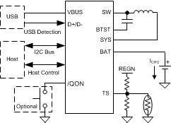
 Simplified Application