-
DRV8703-Q1Functional Safety FIT Rate, FMD and Pin FMA
DRV8703-Q1Functional Safety FIT Rate, FMD and Pin FMA
Trademarks
All trademarks are the property of their respective owners.
1 Overview
This document contains information for DRV8703-Q1 (VQFN (32) package) to aid in a functional safety system design. Information provided are:
- Functional Safety Failure In Time (FIT) rates of the semiconductor component estimated by the application of industry reliability standards
- Component failure modes and their distribution (FMD) based on the primary function of the device
- Pin failure mode analysis (Pin FMA)
DRV8703-Q1 was developed using a quality-managed development process, but was not developed in accordance with the IEC 61508 or ISO 26262 standards.
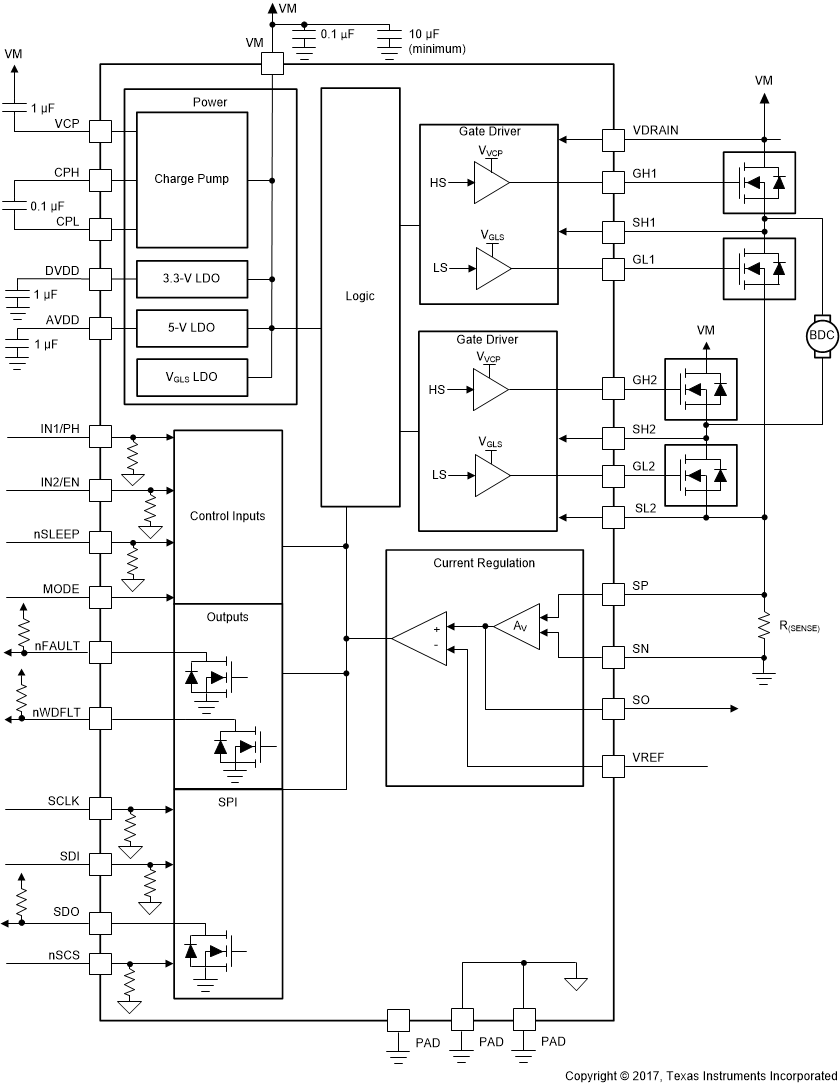
Figure 1-1 shows the device functional block diagram for reference.
 Figure 1-1 Functional Block Diagram
2 Functional Safety Failure In Time (FIT) Rates
This section provides Functional Safety Failure In Time (FIT) rates for DRV8703-Q1 based on two different industry-wide used reliability standards:
- Table 2-1 provides FIT rates based on IEC TR 62380 / ISO 26262 part 11
- Table 2-2 provides FIT rates based on the Siemens Norm SN 29500-2
| FIT IEC TR 62380 / ISO 26262 | FIT (Failures Per 109 Hours) |
|---|---|
| Total Component FIT Rate | 20 |
| Die FIT Rate | 3 |
| Package FIT Rate | 17 |
The failure rate and mission profile information in Table 2-1 comes from the Reliability data handbook IEC TR 62380 / ISO 26262 part 11:
- Mission Profile: Motor Control from Table 11
- Power dissipation: 250 mW
- Climate type: World-wide Table 8
- Package factor (lambda 3): Table 17b
- Substrate Material: FR4
- EOS FIT rate assumed: 0 FIT
| Table | Category | Reference FIT Rate | Reference Virtual TJ |
|---|---|---|---|
| 5 | CMOS, BICMOS, Digital, analog/mixed | 25 FIT | 55 °C |
The Reference FIT Rate and Reference Virtual TJ (junction temperature) in Table 2-2 come from the Siemens Norm SN 29500-2 tables 1 through 5. Failure rates under operating conditions are calculated from the reference failure rate and virtual junction temperature using conversion information in SN 29500-2 section 4.
3 Failure Mode Distribution (FMD)
The failure mode distribution estimation for DRV8703-Q1 in Table 3-1 comes from the combination of common failure modes listed in standards such as IEC 61508 and ISO 26262, the ratio of sub-circuit function size and complexity and from best engineering judgment.
The failure modes listed in this section reflect random failure events and do not include failures due to misuse or overstress.
| Die Failure Modes | Failure Mode Distribution (%) |
|---|---|
| Low side gate turned ON, when commanded OFF | 20.5% |
| Low side gate turned OFF, when commanded ON | 16.0% |
| Low side gate to source voltage too high or too low | 0.5% |
| Low side gate driver slew rate too fast or too slow | 2.5% |
| High side gate turned ON, when commanded OFF | 20.5% |
| High side gate turned OFF, when commanded ON | 15.0% |
| High side gate to source voltage too high or too low | 0.5% |
| High side gate driver slew rate too fast or too slow | 3.5% |
| Dead time between high side FET and low side FET transition incorrect | 1.0% |
| Current sense feedback and regulation incorrect | 6.0% |
| Drain Source voltage monitoring incorrect | 4.0% |
| Incorrect communication or fault indication | 10.0% |
The FMD in Table 3-1 excludes short circuit faults across the isolation barrier. Faults for short circuit across the isolation barrier can be excluded according to ISO 61800-5-2:2016 if the following requirements are fulfilled:
- The signal isolation component is OVC III according to IEC 61800-5-1. If a SELV/PELV power supply is used, pollution degree 2/OVC II applies. All requirements of IEC 61800-5-1:2007, 4.3.6 apply.
- Measures are taken to ensure that an internal failure of the signal isolation component cannot result in excessive temperature of its insulating material.
Creepage and clearance requirements should be applied according to the specific equipment isolation standards of an application. Care should be taken to maintain the creepage and clearance distance of a board design to ensure that the mounting pads of the isolator on the printed-circuit board do not reduce this distance.