Stability Analysis and Design of D-CAP2 and D-CAP3 Converter – Part 2: How to Select Feedforward Capacitor
Trademarks
All trademarks are the property of their respective owners.
1 Introduction
D-CAP series control schemes are widely used in notebook, server, EP power and many other areas due to the advantages of good dynamic performance and less external components [1-2]. The zero formed by output capacitor ESR is used for loop compensation in the original D-CAP control [3- 4]. For some application with small ESR output capacitor, the zero generated by the internal ripple injection circuit can be used for compensation instead of the ESR zero in D-CAP2/D-CAP3 control. In the previous application report https://www.ti.com/lit/pdf/SLVAF11, it is introduced that a simplified method for D-CAP2/D-CAP3 converter stability design is to ensure the ripple injection zero inside bandwidth [5]. On the basis, the output capacitor selection limits are deducted for application design. However, the bandwidth will decrease with increasing output voltage in D-CAP control loop and the ripple injection zero is hard to be kept inside bandwidth. In this condition, the feedforward capacitor, that can provide an additional pair of zero and pole in the loop, can be used to ensure system stability. The detailed analysis and selection method of feedforward capacitor Cff are introduced in this application report.
2 Why We Need Cff in High Output Voltage D-CAP2/3 Converter for Stability
The bode plots of D-CAP2/D-CAP3 converters are shown as Figure 2-1. After the LC double poles frequency ω0 related with inductance and output capacitance, the slope of loop gain can be approximately seen as changing from 0 to -40dB/decade. With the zero injected by the internal ripple injection circuit, the slope becomes – 20dB/decade at 0dB, which could bring sufficient phase margin [7].
 D-CAP2 (b) D-CAP3 Converter") Figure 2-1 Bode Plot
of (a) D-CAP2 (b) D-CAP3 Converter
Figure 2-1 Bode Plot
of (a) D-CAP2 (b) D-CAP3 ConverterFor a stable D-CAP2/3 converter, if output voltage is increased with no other changes, the system will tend to become unstable, as shown in Figure 2-2. Since the gain before double poles frequency equals to Acp*Vref/Vo, system gain and crossover frequency ωcross will decrease with increasing Vo. If ωcross becomes lower than the frequency of ripple injection zero ωRI, system will have a -40dB/decade slope at 0dB, which may cause insufficient phase margin.
 low Vo with
-20dB/Decade Crossing (b) high Vo with
-40dB/Decade Crossing") Figure 2-2 Loop Gain
of a D-CAP2 Converter (a) low Vo with
-20dB/Decade Crossing (b) high Vo with
-40dB/Decade Crossing
Figure 2-2 Loop Gain
of a D-CAP2 Converter (a) low Vo with
-20dB/Decade Crossing (b) high Vo with
-40dB/Decade CrossingFor some D-CAP2/3 converters similar to TPS548D22, the ripple injection zero frequency ωRI is adjustable with external configuration (sometimes named as ramp time constant, the ramp here is the ripple injection, time constant is the reciprocal of angular frequency). For TPS548D22, the Vref can also be adjusted for different output voltage to change ωcross. Those features can both help to adjust the relation of ωcross and ωRI and achieve -20dB/decade crossing.
But for most D-CAP2/3 devices to achieve easy design, the ripple injection zero frequency and reference voltage are fixed. So the LC double poles frequency ω0 must be increased for bandwidth improvement to ensure -20dB/decade slope at 0dB, as shown in Figure 2-3. However, it can be seen from Equation 1 that the inductance and output capacitance must be reduced to increase LC double poles frequency, which will cause large output ripple and noise. That causes the contradiction between output ripple and stability for D-CAP2/3 converters.

 High Vo with
-40dB/Decade Crossing (b) Reducing L or
Co for -20dB/Decade Crossing") Figure 2-3 Loop Gain
of a D-CAP2 Converter (a) High Vo with
-40dB/Decade Crossing (b) Reducing L or
Co for -20dB/Decade Crossing
Figure 2-3 Loop Gain
of a D-CAP2 Converter (a) High Vo with
-40dB/Decade Crossing (b) Reducing L or
Co for -20dB/Decade CrossingIn application report https://www.ti.com/lit/pdf/SLVAF11, TPS568230 was used as an example to illustrate the stability design method for a 1.5 V Vo low output voltage application. Here the case with 5 V Vo is shown to reflect the contradiction between output ripple and stability in high output voltage application.
The condition for analysis is: Vin=12 V, Vo=5 V, Ioutmax=8 A, fsw=600kHz. First, the range of inductance can be got as 1.52uH-3.04uH, according to the principle to limit inductor current ripple as 20%-40% of Ioutmax.
Select inductor 744311220 L=2.2uH. Based on the previous proposed selection method of output capacitor, we could get the limits of Co as 4.7uF-22.3uF. With the upper limit Co=22.3uF, the output voltage ripple is too large to meet the requirement for lots of application.
It is obvious that reducing L or Co is just a trade-off solution between output voltage ripple and stability. Compared to that, adding feedforward capacitor Cff is a better solution to ensure converter stability.
3 Effects of Feedforward Capacitor on the Loop
 Figure 3-1 Scheme of Feedback Divider
Including Feedforward Capacitor
Figure 3-1 Scheme of Feedback Divider
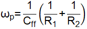
Including Feedforward CapacitorThe effects of adding feedforward capacitor in the feedback divider are studied in the application report [6]. A feedback divider including Cff is shown as Figure 3-1. Cff will introduce a pair of zero and pole in the converter loop. The angular frequency of the introduced zero and pole are:

The effects of the zero and pole introduced by Cff are shown as Figure 3-2.
Cff has both effects on the loop gain and phase. The loop gain is increased to boost bandwidth and optimize transient response. Also, the phase is boosted to increase the phase margin for system stability.
In application notes [2,8], some methods have been proposed to use Cff for phase margin enhancement. But in those methods, the bode plot results without Cff are always needed to get recommended Cff value. That feature makes those Cff selecting methods more applicable in the solution validation process but not in the application design process.
A new method to choose Cff is proposed in this application report. The bode plot results without Cff are not needed to get the recommended Cff value in this method, which makes it more applicable in application design.
