-
UCD9081 8-Channel Power Supply Sequencer and Monitor With Error Logging
- 1 Features
- 2 Applications
- 3 Description
- 4 Revision History
- 5 Pin Configuration and Functions
- 6 Specifications
- 7 Parameter Measurement Information
-
8 Detailed Description
- 8.1 Overview
- 8.2 Functional Block Diagram
- 8.3 Feature Description
- 8.4 Device Functional Modes
- 8.5 Programming
- 8.6 Register Maps
- 9 Application and Implementation
- 10Power Supply Recommendations
- 11Layout
- 12Device and Documentation Support
- 13Mechanical, Packaging, and Orderable Information
- IMPORTANT NOTICE
UCD9081 8-Channel Power Supply Sequencer and Monitor With Error Logging
1 Features
- Single Supply Voltage: 3.3 V
- Low Power Consumption: 3-mA Nominal Supply Current
- Sequences and Monitors Eight Voltage Rails
- Rail Voltages Sampled With 3.2-mV Resolution
- Internal or External Voltage Reference
- Four Configurable Digital Outputs for Power-On-Reset and Other Functions
- Configurable Digital Output Polarity
- Flexible Rail Sequencing Based on Timeline (ms), Parent Rail Regulation Window, or Parent Rail Achieving Defined Threshold
- Independent Under- and Overvoltage Thresholds Per Rail
- Configurable Regulation Expiration Times Per Rail
- Flexible Alarm Processing: Ignore, Log Only, Retry n Times, Retry Continuously, Sequence, Parent Rail Can Shutdown Child Rails
- Alarm Conditions Logged With Timestamp: Under- and Overvoltage Glitch, Sustained Under- and Overvoltage, Rail Did Not Start
- On-Chip Flash for Storing User Data
- Error Logging to Flash for System Failure Analysis
- I2C™ Interface for Configuration and Monitoring
- Microsoft Windows™ GUI for Configuration and Monitoring
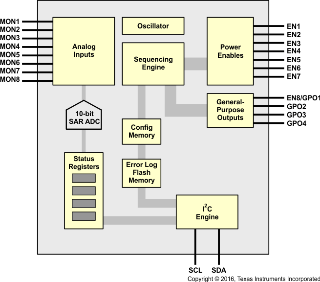
Functional Block Diagram
2 Applications
- Telecommunications Switches
- Servers
- Networking Equipment
- Test Equipment
- Industrial
- Any System Requiring Sequencing of Multiple Voltage Rails
3 Description
The UCD9081 power-supply sequencer controls the enable sequence of up to eight independent voltage rails and provides four general-purpose digital outputs (GPO). The device operates from a 3.3-V supply, provides 3.2-mV resolution of voltage rails, and requires no external memory or clock. The UCD9081 monitors the voltage rails independently and has a high degree of rail sequence and alarm response options. The sequencing of rails can be based on timed events or on timed events in conjunction with other rails achieving regulation or a voltage threshold. In addition, each rail is monitored for undervoltage and overvoltage glitches and thresholds. Each rail the UCD9081 monitors can be configured to shut down a user-defined set of other rails and GPOs, and alarm conditions are monitored on a per-rail basis.
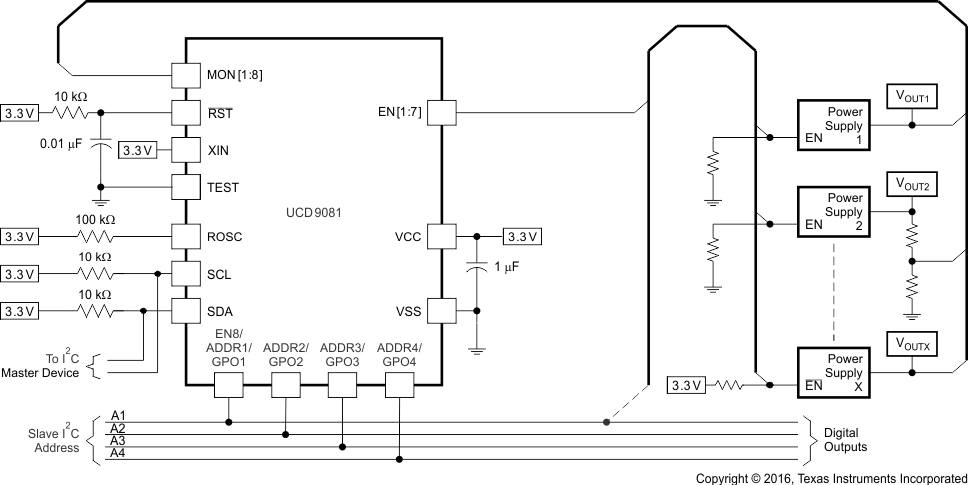
Figure 20 shows the UCD9081 power-supply sequencer in a typical application.
Device Information(1)
| PART NUMBER | PACKAGE | BODY SIZE (NOM) |
|---|---|---|
| UCD9081 | VQFN (32) | 5.00 mm × 5.00 mm |
- For all available packages, see the orderable addendum at the end of the data sheet.
Typical Application Diagram
4 Revision History
Changes from B Revision (December 2010) to C Revision
- Added ESD Ratings table, Feature Description section, Device Functional Modes, Application and Implementation section, Power Supply Recommendations section, Layout section, Device and Documentation Support section, and Mechanical, Packaging, and Orderable Information sectionGo
- Deleted Ordering Information table; see POA at the end of the data sheetGo
- Added Thermal Information tableGo
- Moved Timing Parameters for I2C Interface table and I2C Timing diagram to SpecificationsGo
- Moved content in Monitoring the UCD9081 to Register MapsGo
Changes from A Revision (September 2008) to B Revision
- Added Note 1 to the PIN FUNCTIONS tableGo
- Added Note regarding state of enable and digital I/O pins when the device contains factory configurationGo
- Added a reference to the UCD9081 Programming GuideGo
Changes from * Revision (June 2008) to A Revision
5 Pin Configuration and Functions
Pin Functions
| PIN(1) | I/O | DESCRIPTION | |
|---|---|---|---|
| NAME | NO. | ||
| ADDR2/GPO2 | 26 | I/O | I2C address select 2, general-purpose digital output 2 |
| ADDR3/GPO3 | 27 | I/O | I2C address select 3, general-purpose digital output 3 |
| ADDR4/GPO4 | 28 | I/O | I2C address select 4, general-purpose digital output 4 |
| EN1 | 23 | I/O | Voltage rail 1 enable (digital output) |
| EN2 | 24 | I/O | Voltage rail 2 enable (digital output) |
| EN3 | 11 | I/O | Voltage rail 3 enable (digital output) |
| EN4 | 10 | I/O | Voltage rail 4 enable (digital output) |
| EN5 | 12 | I/O | Voltage rail 5 enable (digital output) |
| EN6 | 13 | I/O | Voltage rail 6 enable (digital output) |
| EN7 | 14 | I/O | Voltage rail 7 enable (digital output) |
| EN8/ADDR1/ GPO1 |
25 | I/O | Voltage rail 8 enable (digital output), I2C address select 1, general-purpose digital output 1 |
| MON1 | 6 | I | Analog input for voltage rail 1 |
| MON2 | 7 | I | Analog input for voltage rail 2 |
| MON3 | 8 | I | Analog input for voltage rail 3 |
| MON4 | 18 | I | Analog input for voltage rail 4 |
| MON5 | 19 | I | Analog input for voltage rail 5 |
| MON6 | 9 | I | Analog input for voltage rail 6 |
| MON7 | 15 | I | Analog input for voltage rail 7 |
| MON8 | 16 | I | Analog input for voltage rail 8 |
| NC | 2 | — | Do not connect |
| NC | 4, 17, 20, 31 |
— | Recommended to connect to VSS, pin is not connected internally |
| ROSC | 32 | — | Internal oscillator frequency adjust. Must use 100-kΩ pullup to VCC for minimum drift and maximum frequency when sampling voltage rails. |
| RST | 5 | I | Reset input |
| SCL | 22 | I/O | I2C clock. Must pull up to 3.3 V. |
| SDA | 21 | I/O | I2C data. Must pull up to 3.3 V. |
| TEST | 29 | I | Connect to VSS |
| VCC | 30 | — | Supply voltage |
| VSS | 1 | — | Ground reference |
| XIN | 3 | — | Connect to VCC |
| PowerPAD™ | — | — | Package pad. Recommended to connect to VSS. |
6 Specifications
6.1 Absolute Maximum Ratings
over operating free-air temperature range (unless otherwise noted)(1)| MIN | MAX | UNIT | |
|---|---|---|---|
| Voltage applied from VCC to VSS | –0.3 | 4.1 | V |
| Voltage applied to any pin(2) | –0.3 | VCC + 0.3 | V |
| ESD diode current at any device terminal | ±2 | mA | |
| Storage temperature, Tstg | –40 | 85 | °C |
6.2 Recommended Operating Conditions
| MIN | NOM | MAX | UNIT | ||
|---|---|---|---|---|---|
| VCC | Supply voltage during operation and configuration changes | 3 | 3.3 | 3.6 | V |
| TA | Operating free-air temperature | –40 | 85 | °C | |
6.3 Thermal Information
| THERMAL METRIC(1) | UCD9081 | UNIT | |
|---|---|---|---|
| RHB (VQFN) | |||
| 32 PINS | |||
| RθJA | Junction-to-ambient thermal resistance | 32.1 | °C/W |
| RθJC(top) | Junction-to-case (top) thermal resistance | 18.1 | °C/W |
| RθJB | Junction-to-board thermal resistance | 6 | °C/W |
| ψJT | Junction-to-top characterization parameter | 0.2 | °C/W |
| ψJB | Junction-to-board characterization parameter | 5.9 | °C/W |
| RθJC(bot) | Junction-to-case (bottom) thermal resistance | 1.2 | °C/W |
6.4 Electrical Characteristics
These specifications are over recommended ranges of supply voltage and operating free-air temperature (unless otherwise noted)| PARAMETER | TEST CONDITIONS | MIN | TYP | MAX | UNIT | ||
|---|---|---|---|---|---|---|---|
| SUPPLY CURRENT | |||||||
| IS | Supply current into VCC | TA = 25°C, excluding external current | 3 | 4 | mA | ||
| IC | Supply current during configuration | VCC = 3.6 V | 3 | 7 | mA | ||
| STANDARD INPUTS (RST, TEST) | |||||||
| VIL | Low-level input voltage | VCC = 3 V | VSS | VSS + 0.6 | V | ||
| VIH | High-level input voltage | VCC = 3 V | 0.8 × VCC | VCC | V | ||
| SCHMITT TRIGGER INPUTS (SDA, SCL, EN[1...7], EN8/ADDR1, ADDR[2...4]) | |||||||
| VIT+ | Positive-going input threshold voltage | VCC = 3 V | 1.5 | 1.9 | V | ||
| VIT– | Negative-going input threshold voltage | VCC = 3 V | 0.9 | 1.3 | V | ||
| Vhys | Input voltage hysteresis | VCC = 3 V, VIT+ – VIT– | 0.5 | 1 | V | ||
| Ilkg | High-impedance leakage current | ±50 | nA | ||||
| ANALOG INPUTS (MONx, ROSC) | |||||||
| VCC | Analog supply voltage | VSS = 0 V | 3 | 3.6 | V | ||
| VMON<1..8> | Analog input voltage | Internal voltage reference selected | 0 | 2.5 | V | ||
| External voltage reference selected (VCC used as reference) |
0 | VCC | |||||
| CI(1) | Input capacitance | Only one terminal can be selected at a time (MON1 to MON8) | 27 | pF | |||
| RI(1) | Input MUX ON resistance | 0 V ≤ VMONx ≤ VCC, VCC = 3 V | 2000 | Ω | |||
| Ilkg | High-impedance leakage current | MON1 to MON8 | ±50 | nA | |||
| VREF+ | Positive internal reference voltage | Internal voltage reference selected, VCC = 3 V |
2.35 | 2.5 | 2.65 | V | |
| VTUE | ADC total unadjusted error | VCC = 3 V | VR+ = 2.5 V (internal reference) |
±12.2 | mV | ||
| VR+ = VCC
(external reference) |
±14.7 | ||||||
| TREF+(1) | Temperature coefficient of internal voltage reference | I(VREF+) is a constant in the range of 0 mA ≤ I(VREF+) ≤ 1 mA, VCC = 3 V |
±100 | ppm/°C | |||
| MISCELLANEOUS | |||||||
| Tretention | Retention of configuration parameters | TJ = 25°C | 100 | Years | |||
| POR, BROWNOUT, RESET(4)(5) | |||||||
| td(BOR) | Brownout | 2000 | µs | ||||
| VCC(start) | Brownout | dVCC/dt ≤ 3 V/s | 0.7 × V(B_IT–) | V | |||
| V(B_IT–) | Brownout | dVCC/dt ≤ 3 V/s | 1.71 | V | |||
| Vhys(B_IT–) | Brownout | dVCC/dt ≤ 3 V/s | 70 | 130 | 180 | mV | |
| t(reset) | Brownout | Pulse length required at RST pin to accept reset internally, VCC = 3 V | 2 | µs | |||
| DIGITAL OUTPUTS (EN8/GPO1, GPO[2...4], EN[1...7], SDA, SCL) | |||||||
| VOH | High-level output voltage | IOHmax = –1.5 mA(2), VCC = 3 V | VCC – 0.25 | VCC | V | ||
| IOHmax = –6 mA(3), VCC = 3 V | VCC – 0.6 | VCC | |||||
| VOL | Low-level output voltage | IOLmax = 1.5 mA(2), VCC = 3 V | VSS | VSS + 0.25 | V | ||
| IOLmax = 6 mA(3), VCC = 3 V | VSS | VSS + 0.6 | |||||
| Ilkg | High-impedance leakage current | VCC = 3 V | ±50 | nA | |||
6.5 Timing Requirements: I2C Interface
| MIN | MAX | UNIT | ||
|---|---|---|---|---|
| tofof | Output fall time from VOH to VOL(1) with a bus capacitance from 10 pF to 400 pF | 250(2) | ns | |
| CI | Capacitance for each pin | 10 | pF | |
| fSCL | SCL clock frequency | 10 | 100 | kHz |
| tHD;STA | Repeated hold time START condition (after this period, the first clock pulse is generated) | 4 | µs | |
| tHD;DAT | Data hold time | 0(3) | 3.45(4) | µs |
| tLOW | LOW period of the SCL clock | 4.7 | µs | |
| tHIGH | HIGH period of the SCL clock | 4 | µs | |
| tSU;STA | Setup time for repeated start condition | 4.7 | µs | |
| tSU;DAT | Data setup time | 250 | ns | |
| tr | Rise time of both SDA and SCL signals | 1000 | ns | |
| tf | Fall time of both SDA and SCL signals | 300 | ns | |
| tSU;STO | Setup time for STOP condition | 4 | µs | |
| tBUF | Bus free time between a STOP and START condition | 4.7 | µs | |
| C(b) | Capacitive load for each bus line | 400 | pF | |
| VnL | Noise margin at the LOW level for each connected device (including hysteresis) | 0.1 × VDD | V | |
| VnH | Noise margin at the HIGH level for each connected device (including hysteresis) | 0.2 × VDD | V | |
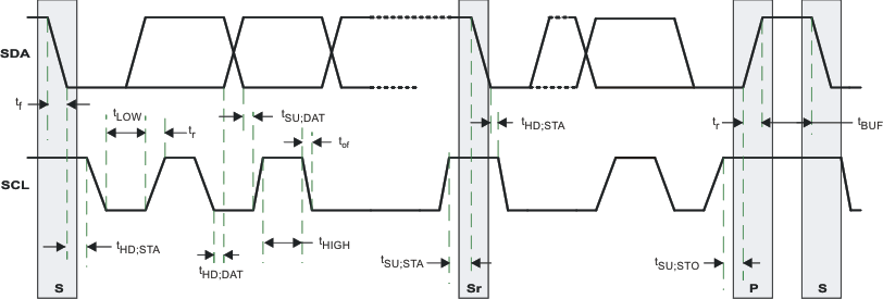 Figure 1. Timing Diagram for I2C Interface
6.6 Typical Characteristics
Digital outputs (only one output is loaded at a time)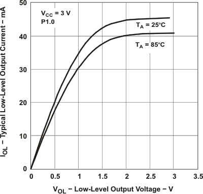 Figure 2. Typical Low-Level Output Current
vs Low-Level Output Voltage
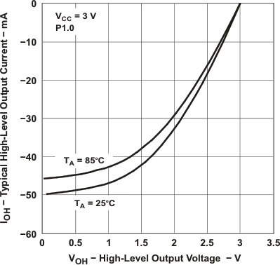 Figure 3. Typical High-Level Output Current
vs High-Level Output Voltage
7 Parameter Measurement Information
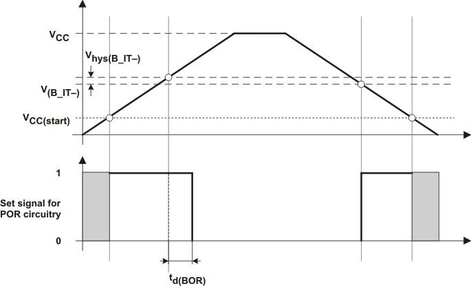 Figure 4. POR/Brownout Reset (BOR) vs Supply Voltage
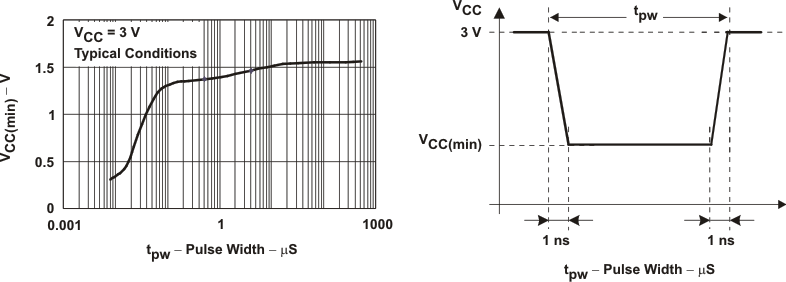 Figure 5. VCC(min) Level With a Square Voltage Drop to Generate a POR/Brownout Signal
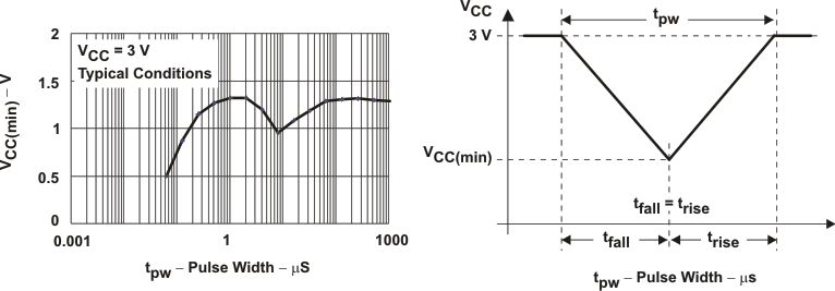 Figure 6. VCC(min) Level With a Triangle Voltage Drop to Generate a POR/Brownout Signal