-
Power Stage Designer
- Abstract
- Trademarks
- 1 Topologies Window
- 2 FET Losses Calculator
- 3 Load Step Calculator
- 4 Capacitor Current Sharing Calculator
- 5 AC/DC Bulk Capacitor Calculator
- 6 RCD-Snubber Calculator for Flyback Converters
- 7 RC-Snubber Calculator
- 8 Output Voltage Resistor Divider
- 9 Dynamic Analog Output Voltage Scaling
- 10Dynamic Digital Output Voltage Scaling
- 11Unit Converter
-
12Loop Calculator
- 12.1 Inputs
- 12.2
Transfer Functions
- 12.2.1 Output Impedance Transfer Function
- 12.2.2 Transfer Function VMC Buck Power Stage
- 12.2.3 Transfer Function CMC Buck Power Stage
- 12.2.4 Transfer Function CMC Boost Power Stage
- 12.2.5 Transfer Function CMC Inverting Buck-Boost Power Stage
- 12.2.6 Transfer Function CMC Forward Power Stage
- 12.2.7 Transfer Function CMC Flyback Power Stage
- 12.2.8 Transfer Function Closed Loop
- 12.2.9 Transfer Function Isolated Type II Compensation Network With a Zener Clamp
- 12.2.10 Transfer Function Isolated Type II Compensation Network Without a Zener Clamp
- 13Filter Designer
- 14Additional Information
- 15Revision History
- IMPORTANT NOTICE
Power Stage Designer
1 Abstract
Power Stage Designer™ software tool is a Java® based tool that helps engineers speed up their power supply designs by calculating voltages and currents for 21 topologies according to the user's inputs. Additionally, Power Stage Designer contains a Bode plotting tool and a helpful toolbox with various functions for power supply design. This document describes how the different features of Power Stage Designer can be used and also explains the calculations behind these functions.
Trademarks
Power Stage Designer™ is a trademark of Texas Instruments.
Java® is a registered trademark of Oracle.
All trademarks are the property of their respective owners.
1 Topologies Window
To start a power supply design with Power Stage Designer, first select a topology from the Topology menu. The window changes and displays the schematic of the selected topology with a set of input fields and various output values. After entering the parameters of the power supply specification, Power Stage Designer suggests a value for the output inductance to stay below the entered current ripple requirement. For isolated topologies, the tool also displays a recommendation for the transformer turns ratio (TTR) based on the selected maximum duty cycle and suggests a value for the magnetizing inductance. Users can enter values of their choice and evaluate their impact on voltage and current waveforms and other parameters like on-time, off-time, and duty cycle.
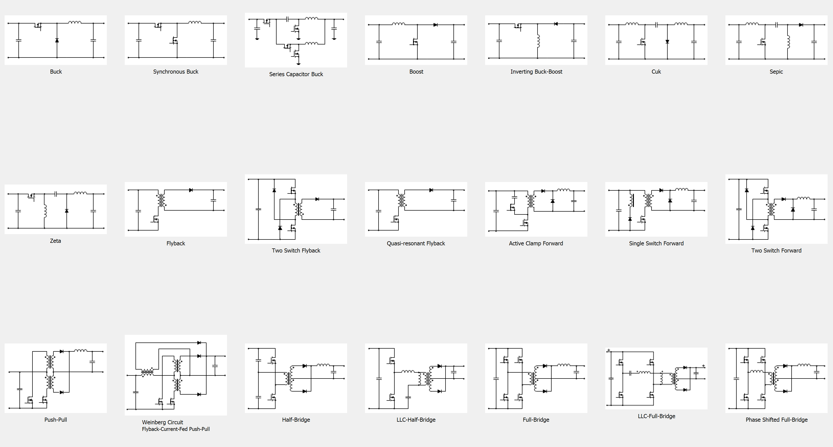
#SLVUBB49830 shows the main window of Power Stage Designer displaying supported topologies.
 Figure 1-1 Main
Window of Power Stage Designer Displaying Supported Topologies
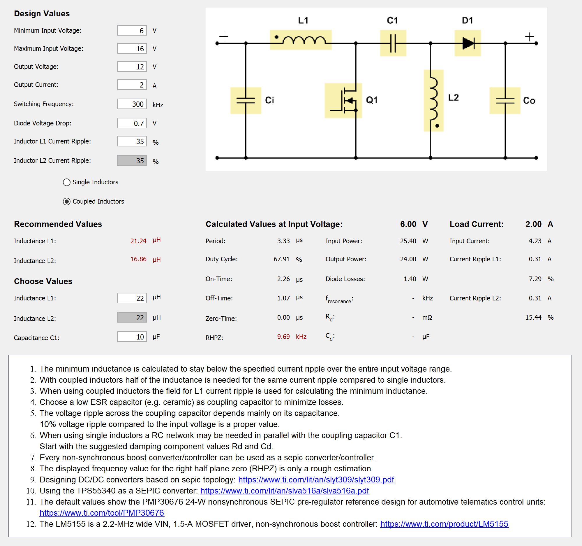
 Figure 1-2 Topology
Window for SEPIC
Figure 1-2 Topology
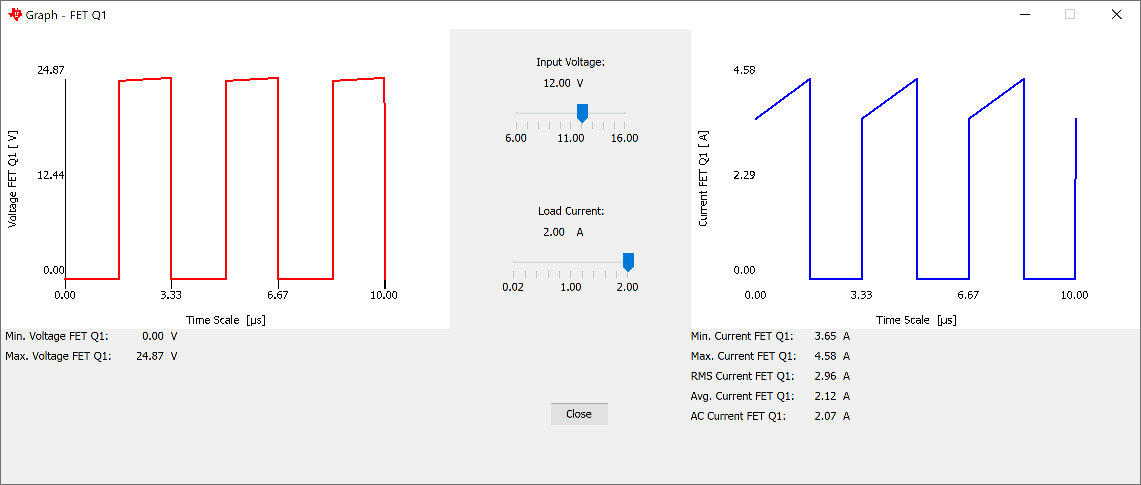
Window for SEPICAfter clicking on one of the yellow highlighted components in the schematic (see #SLVUBB42919), a new window displays the voltage and current waveforms for this specific component (see #SLVUBB45520). Additional information like the minimum and maximum voltage, minimum and maximum current, as well as root mean square (RMS), average, and AC values for the current is also provided in this window. The input voltage can be changed across the entire input voltage range with a slider. For most topologies the load current can be altered in the range of 1% to 100% of the entered output current with a second slider. Some topology models do not support such a wide load current range, thus the load current slider can be changed only in the range of 50% and 100%. The Quasi-resonant Flyback model uses a fixed output power as base for all calculations. That is why the load current slider is not available for this specific topology.
 Figure 1-3 Graph
Window for FET Q1 of a SEPIC Operating in CCM
Figure 1-3 Graph
Window for FET Q1 of a SEPIC Operating in CCMAll equations used for calculations are ideal, with the only exception that the forward voltage of rectifier and freewheeling diodes is considered. For a collection of the equations behind certain topologies, see the Power Topologies Handbook.
2 FET Losses Calculator
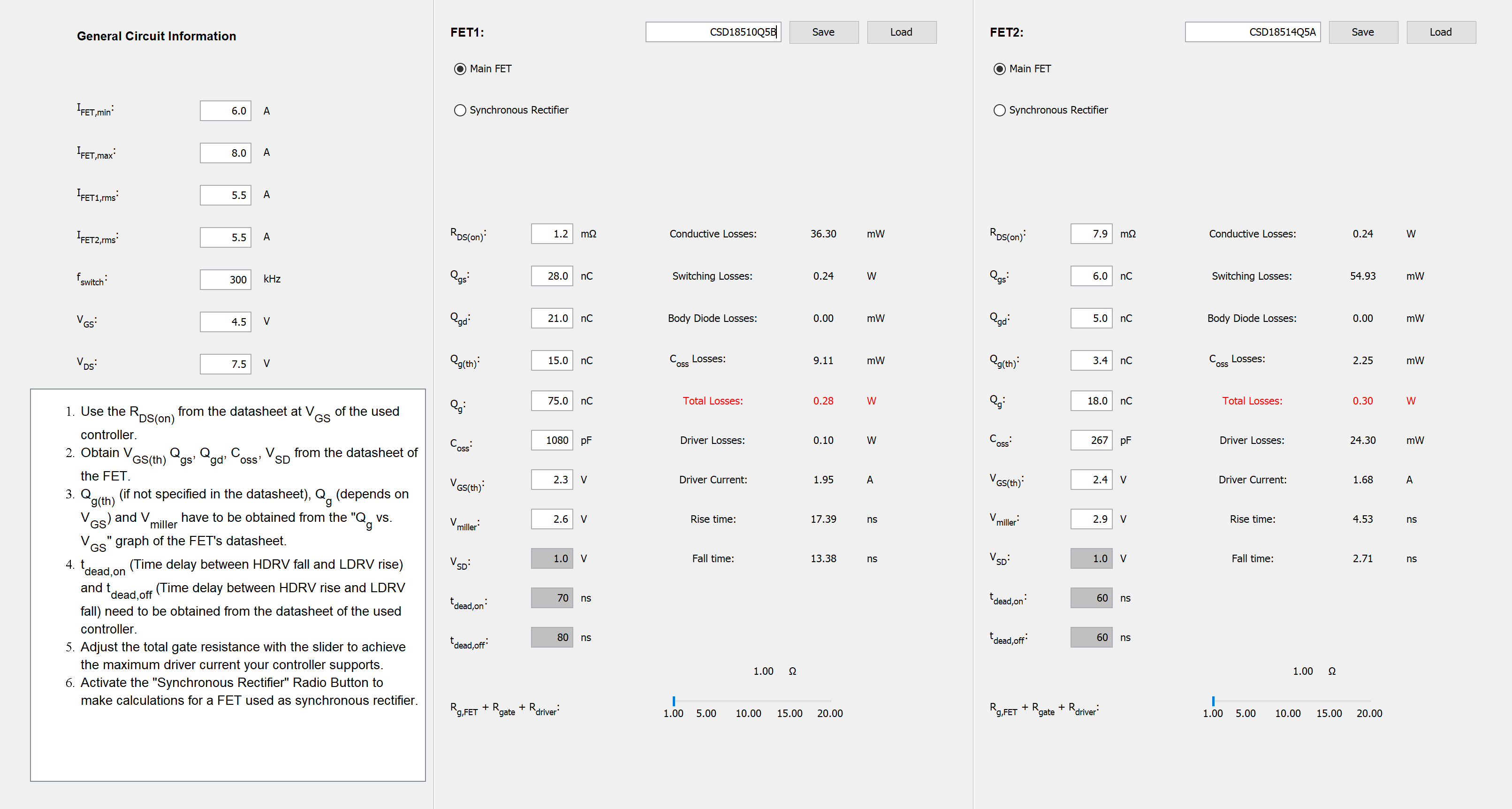
The FET Losses Calculator lets the user either compare two different FETs or calculate losses for the main FET and a synchronous rectifier in a hard-switching power stage. #SLVUBB44807 shows the FET Losses Calculator window.
The Quasi-resonant Flyback, LLC-Half-Bridge, LLC-Full-Bridge, and Phase-Shifted Full-Bridge are resonant topologies. Manual inputs can provide more accurate results.
 Figure 2-1 FET
Losses Calculator Window
Figure 2-1 FET
Losses Calculator WindowTo attain the most accurate results, it is important to determine the gate drive voltage (VGS) of the power management controller since the values for Qg (which is relevant for driver losses) and RDS(on) are dependent on this voltage and must be obtained from graphs in the data sheet of the FET.
The different losses which can be seen in the FET of a power supply are conducted losses, switching losses, Coss losses, and body diode losses. Reverse recovery losses are neglected, but can become significant at high switching frequencies.
Conductive losses:
Switching losses:
Coss losses:
Body Diode losses:
The total losses for the main FET can be calculated as indicated in #SLVUBB44493
For synchronous rectifiers, the switching losses equal zero due to soft switching, but during the dead time the body diode is conducting. So the total losses result as indicated in #SLVUBB48072:
Additionally, driver losses occur in the power management controller, which can be calculated as shown in #SLVUBB44947:
Power management controllers typically have a limited amount of gate drive current they can source and sink. Therefore, it is important to adjust the total resistance in the gate drive path so the resulting gate drive current is equal to or smaller than the limit in the data sheet.