-
BOOSTXL-TPS65033 User's Guide
- Trademarks
- 1BOOSTXL-TPS65033 Components and Environment
- 2BOOSTXL-TPS65033 Board Information
- 3Programming GUI Operation
- 4Recommended Operating Procedure
- 5BOOSTXL-TPS65033 Schematic
- 6BOOSTXL-TPS65033 Board Layers
- 7BOOSTXL-TPS65033 Bill of Materials
- 8Revision History
- IMPORTANT NOTICE
BOOSTXL-TPS65033 User's Guide
Trademarks
Google Chrome is a trademark of Google, LLC.
Mozilla Firefox is a trademark of Mozilla Foundation.
Windows is a registered trademark of Microsoft Corporation.
macOS is a registered trademark of Apple Inc.
Linux is a registered trademark of The Linux Foundation.
All other trademarks are the property of their respective owners.
1 BOOSTXL-TPS65033 Components and Environment
The TPS65032001-Q1 and TPS65033x-Q1 family of PMICs are configurable and programmable only through I2C instructions. The BOOSTXL-TPS65033 socketed board is designed to act as a BoosterPack to the low cost TI LaunchPads, enabling a LaunchPad to act as the USB-to-I2C interface for communication with a personal computer. This separation reduces the cost of prototyping and enables experimentation with various TI devices, including custom software development using existing LaunchPad tools. Many of these tools can be found online at TI DevTools. The programming GUI is also available in the TI DevTools Gallery. This GUI is compatible with both the MSP430F5529LP and the MSP432E401Y LaunchPads.
2 BOOSTXL-TPS65033 Board Information
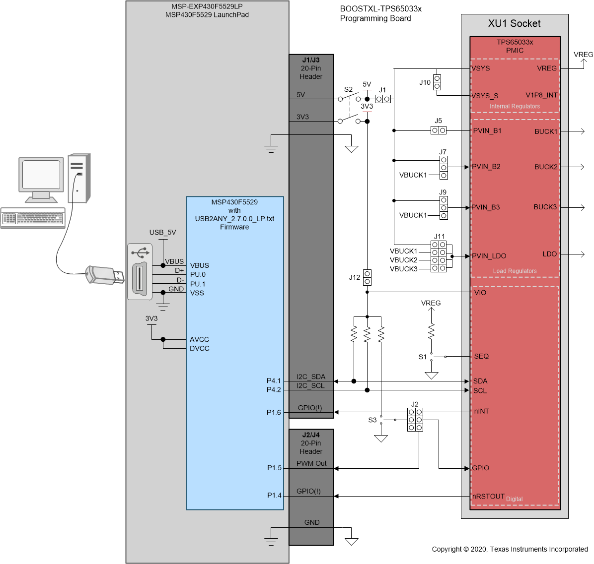
The BOOSTXL-TPS65033 is designed to stack on top of a LaunchPad, connecting the relevant power and MCU pins to the PMIC through the headers J1/J3 and J2/J4. Power is delivered to the PMIC from the USB port of a PC through the the LaunchPad 5 V and 3.3 V rails. The following block diagram demonstrates how the LaunchPad interfaces with the PC and the PMIC.
 Figure 2-1 Programming Board and LaunchPad
Connections
Figure 2-1 Programming Board and LaunchPad
Connections2.1 Critical Socketed Board Connections
Critical connections for operating the socketed board are the 5 V rail, the 3.3 V rail, and the I2C pins. The remaining connections to the LaunchPad are left available for future experimentation. Note: I2C pull-ups must be pulled up to VIO. This can optionally be pulled up to 3.3 V (default) or an alternate rail through the J12.
By default, the 3.3 V rail must be present to power the VIO and GPIO pins to fully enable the PMIC. If evaluation without a PC is desired, both the 5 V and the VIO domains should be externally supplied. If VIO is supplied by a voltage other than 3.3 V, J12 should be left open to prevent potential current paths to the MCU 3.3 V. For most configurations, the PMIC can supply VIO when externally connected to an appropriate test point, for example the Buck 1 output if configured for 3.3 V, or the Buck 2 output if configured for 1.8 V.
2.1.1 Power Switches
Both the 5 V and 3.3 V rails connect to the PMIC through separate current limiting load switches. The load switches are simultaneously enabled with the S2 toggle switch on the top left area of the board. See Section 5 for the complete BOOSTXL-TPS65033 schematic. It is recommended to keep S2 open when connecting the LaunchPad to the PC to reduce the initial current draw from the USB port.