-
Achieving high converter efficiency with an active clamp in a PSFB converter
Achieving high converter efficiency with an active clamp in a PSFB converter
1 Introduction
Phase-shifted full-bridge (PSFB) converters (see Figure 1-1) are widely applied to high-power applications, mainly because a PSFB converter can achieve soft switching on its input switches and thus facilitate high converter efficiency [1]. Although soft switching greatly reduces switching losses, the output rectifier parasitic capacitance resonates with the transformer leakage inductors – modeled as Lr in Figure 1-1 – resulting in voltage ringing with high voltage stress [2].
The voltage stress of the output rectifier could be as high as 2 x VIN x NS/NP, where NP and NS are the transformer’s primary and secondary windings, respectively. Traditionally, applying a passive snubber [2] (such as the resistor-capacitor-diode [RCD] snubber in Figure 1-1) at the output rectifier prevents the rectifier voltage from going too high and enables the use of a lower-voltage-rated component with a better figure of merit for lower power dissipation.
When applying metal-oxide semiconductor field-effect transistors (MOSFETs) as a synchronous rectifier (SR), you can expect lower Coss and RDS(on) on lower-voltage-rated MOSFETs at the same cost level compared to higher-voltage-rated MOSFETs. However, using a passive snubber means that part of the energy that caused the voltage ringing will dissipate in the passive snubber and result in an efficiency reduction.
This article introduces an active (rather than a passive) snubber and its related control, which minimizes rectifier voltage stress to achieve higher converter efficiency while also greatly reducing energy dissipation in the snubber circuit and without sacrificing operational range.
2 A PSFB converter with an active clamp
As shown in Figure 2-1, inserting an active clamp leg formed by a capacitor (CCL) and a MOSFET (QCL) before the output inductor enables active clamp leg current conduction within the effective duty-cycle (Deff) period, thus clamping the secondary winding voltage (VSEC) and rectifier voltage stress to the CCL voltage – VCL. In order to have low voltage stress on the output rectifier, you must select a large-enough CCL for low capacitor voltage ripple. A rule of thumb is to select the inductor-capacitor (LC) resonant period formed by Lr and CCL to be much longer than the switching period (Ts) [3] expressed by Equation 1:
The rectifier voltage stress will clamp to around VINx NS/NP with the active snubber, which is about half of the voltage stress without any clamp circuit.
Unlike a passive snubber, an active snubber doesn’t dissipate the ringing energy on the power resistor. Instead, it circulates the energy in the LC resonant tank as a lossless snubber. When the output winding voltage becomes nonzero, energy will transfer from the primary winding to the secondary winding to energize the output inductor and conduct current through the QCL body diode, even if QCL isn’t turned on. Turning on QCL after its body has already conducted current will ensure zero voltage switching (ZVS) on QCL. Therefore, you can expect higher converter efficiency on a PSFB converter with an active snubber over a PSFB converter with a passive snubber in an identical specification.
3 Active clamp leg design considerations
With the active snubber implemented in a PSFB, the transformer winding current will no longer rise monotonically during the effective duty cycle (Deff) period (TS) (non-zero output winding voltage period) like output inductor current. This is because the active snubber capacitor energy also participates in energizing output inductor rather than solely rely on energy transfer from the input side. The non-monotonic current ramp characteristic could make peak current mode control difficult as input or transformer winding current are generally utilized for peak current detection and higher input or transformer winding current does not necessarily represent larger duty cycle.
In order to allow peak current detection happens when current is rising monotonically, we must ensure DeffTS is always greater than the duration where current-second balance is completed – DCSBTS – under whole operational voltage and load ranges. As high efficiency is expected for a PSFB with larger Deff, PSFB is generally designed to have larger Deff at mid-to-heavy load where Deff >> DCSB is expected. At light load, converter is expected to operate under discontinuous conduction mode where Deff will be smaller than Deff under continuous conduction mode at the same input/output voltage condition. In order to keep DeffTS greater than DCSBTS even at light load, we have implemented frequency reduction control based on load current.
The duration of DCSBTS becomes an important factor for peak current mode control. How long does it take to complete current-second balance is now the one-million-dollar question. To answer this question, you’ll need to calculate current flow through the active clamp leg.
Assuming that VCL is a constant and Lm = ∞, Equation 2 expresses the rectifier current changing rate during the duty-cycle loss period (the period where VSEC = 0 and iSR1 and iSR2 are commuting) as:
where VLr is the voltage across Lr.
Equation 3 calculates the changing rate of the output inductor current:
Using Equation 2 and Equation 3 along with Kirchhoff’s current law, Equation 4 calculates the changing rate of the active clamp current:
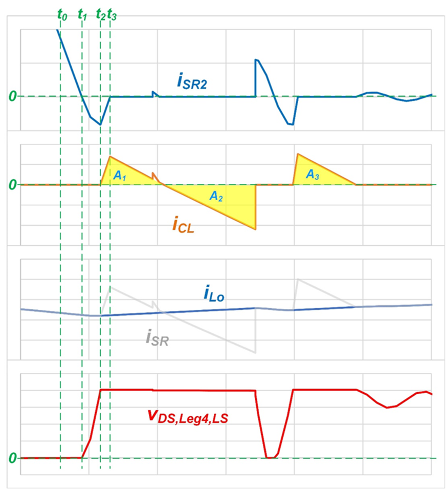
Since VCL ≈ VIN x NS/NP [3], you just need to apply the total active clamp leg conduction time as Δt in Equation 4 to solve ΔiCL. However, you still need to know the peak value of iCL in order to calculate the iCL root-mean-square (RMS) value. As shown in Figure 3-1, if iSEC = iLo (after charging Coss to VCL) at time t2 and iSEC = iSR at time t3 (start to charge CCL), Equation 5 derives iCL,peak as:
 Figure 3-1 Key waveforms around the
active clamp current conduction period.
Figure 3-1 Key waveforms around the
active clamp current conduction period.With Equation 6 deriving the iSR2 value at t2 as:
Assuming that the iSR2 current decreasing rate from t0 to t2 is the same, Equation 7 derives the time duration of t2-t1 as:
Since CLneeds to maintain a current second balance, the sum of areas A1 and A3 will equal area A2.
As shown in Equation 7, SR Coss controls the peak current on the active clamp leg. If you select a low Coss SR FET, the active clamp leg RMS current is lower and thus helps improve converter efficiency.
Here are some design guidelines when designing a PSFB converter with an active snubber:
- QCL must turn on only after the duty-cycle loss duration in order to avoid CCL energy backflow to the primary side.
- QCL must be turn on while the body diode is still conducting current for ZVS.
- A longer QCL on time will reduce VCL as well as SR voltage stress, but the QCL RMS current will increase.
- A lower SR Coss will not only help reduce the active clamp leg RMS current, but also help reduce SR voltage stress.
The active clamp method isn’t limited to full-bridge rectifiers; it is applicable to other types of rectifiers such as current-doubler [4] or center-taped rectifiers. Figure 3-2 shows a PSFB converter with an active clamp on a center-taped rectifier, which is implemented in the 3-kW Phase-Shifted Full Bridge with Active Clamp Reference Design with >270-W/in3 Power Density.
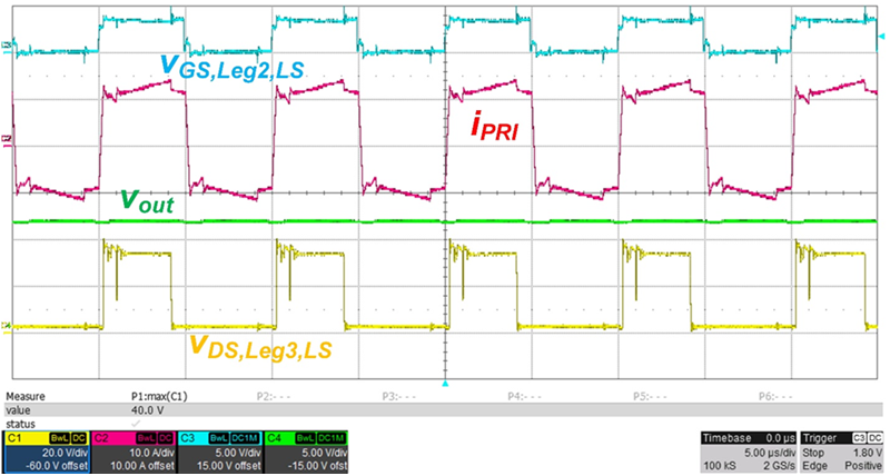
As shown in Figure 3-3, it is possible to clamp SR voltage stress under 40 V with dual active clamp legs, with negligible clamping loss (very minor conduction loss) at a 250-A load current.
 Figure 3-3 Steady-state waveform of a
PSFB converter with a center-taped rectifier and active snubbers at a 12-V/3-kW
output.
Figure 3-3 Steady-state waveform of a
PSFB converter with a center-taped rectifier and active snubbers at a 12-V/3-kW
output.4 Summary
A control method allows PSFB converter to work with active snubber under peak current mode control is discussed in this paper. The active snubber allows lower voltage stress on the output rectifier with negligible power dissipation on the snubber circuit that greatly improves converter efficiency. The current disturbance introduced by the active snubber makes peak current mode control difficult. With the active snubber power switch on-time fixed and frequency reduction control implemented, a high efficiency and peak current controlled PSFB converter can be realized. A 400Vin, 12Vout/3kW PSFB prototype is built with the proposed control method has been verified across whole operational load range with output rectifier voltage stress limited below 40 V at 250A full load.
5 References
- Designing a Phase Shifted Zero Voltage Transition (ZVT) Power Converter. Unitrode Power Supply Design Seminar SEM 900, 1993.
- Lin, Song-Yi, and Chern-Lin Chen. April 1998. “Analysis and Design for RCD Clamped Snubber Used in Output Rectifier of Phase-Shift Full-Bridge ZVS Converters.” Published in IEEE Transactions on Industrial Electronics 45 (2), pp. 358-359.
- Sabate, J.A., V. Vlatkovic, R.B. Ridley, and F.C. Lee. 1991. “High-Voltage, High-Power, ZVS, Full-Bridge PWM Converter Employing an Active Snubber.” Sixth Annual Applied Power Electronics Conference and Exhibition, pp. 158-163.
- Texas Instruments: Design Review: 100W, 400kHz, DC/DC Converter With Current Doubler Synchronous Rectification Achieves 92% Efficiency.
IMPORTANT NOTICE AND DISCLAIMER
TI PROVIDES TECHNICAL AND RELIABILITY DATA (INCLUDING DATASHEETS), DESIGN RESOURCES (INCLUDING REFERENCE DESIGNS), APPLICATION OR OTHER DESIGN ADVICE, WEB TOOLS, SAFETY INFORMATION, AND OTHER RESOURCES “AS IS” AND WITH ALL FAULTS, AND DISCLAIMS ALL WARRANTIES, EXPRESS AND IMPLIED, INCLUDING WITHOUT LIMITATION ANY IMPLIED WARRANTIES OF MERCHANTABILITY, FITNESS FOR A PARTICULAR PURPOSE OR NON-INFRINGEMENT OF THIRD PARTY INTELLECTUAL PROPERTY RIGHTS.
These resources are intended for skilled developers designing with TI products. You are solely responsible for (1) selecting the appropriate TI products for your application, (2) designing, validating and testing your application, and (3) ensuring your application meets applicable standards, and any other safety, security, or other requirements. These resources are subject to change without notice. TI grants you permission to use these resources only for development of an application that uses the TI products described in the resource. Other reproduction and display of these resources is prohibited. No license is granted to any other TI intellectual property right or to any third party intellectual property right. TI disclaims responsibility for, and you will fully indemnify TI and its representatives against, any claims, damages, costs, losses, and liabilities arising out of your use of these resources.
TI’s products are provided subject to TI’s Terms of Sale (www.ti.com/legal/termsofsale.html) or other applicable terms available either on ti.com or provided in conjunction with such TI products. TI’s provision of these resources does not expand or otherwise alter TI’s applicable warranties or warranty disclaimers for TI products.
Mailing Address: Texas Instruments, Post Office Box 655303, Dallas, Texas 75265
Copyright © 2023, Texas Instruments Incorporated