Clocking Optimization for RF Sampling Analog-to-Digital Converters
Trademarks
All trademarks are the property of their respective owners.
1 ADC Signal-to-Noise Ratio Components
The signal-to-noise ratio (SNR) of the ADC is a key specification. A high number for this specification indicates the ADC can better distinguish the desired input signal from the undesired noise that is also captured during sampling. There are three main contributors to the SNR of an ADC, the quantization and thermal noise of the ADC (does not change with input frequency) and the clock jitter (depends on the frequency). Figure 1-1 shows an example of an ADC thermal noise of 62.5 dBFs and the SNR of the clock (with a jitter, tclock_jitter of 50 fs). The SNR of a clock can be derived from knowing the frequency of the signal and the jitter (discussed in Section 2) with Equation 1:
As the figure illustrates, the high SNR of the ADC is maintained for the low input frequencies, but starts to be dominated by the clock SNR at higher input frequencies.
 Figure 1-1 ADC
and Clock Jitter Contribution to SNR
Figure 1-1 ADC
and Clock Jitter Contribution to SNRNow that the impact of clock jitter to the total SNR when the clock has a jitter of 50 fs is known, look at the impact of lower performance clock (with higher jitter). As Figure 1-2 shows, the higher the jitter of the clock, the more severe the effect of degradation in SNR from the clock performance at higher ADC input frequencies. Therefore, it is essential to make sure the clock jitter is the lowest possible, and this specification can be adjusted according to different parameters of a high frequency synthesizer clock source to achieve the optimal low jitter value.
 Figure 1-2 Impact of Different Clock Jitter to Total SNR
2 Understanding Phase Noise and Jitter and SNR
Designing for and finding out the lowest jitter starts from knowing the phase noise of a clock signal from a synthesizer. In the time domain, an ideal sine-wave clock signal looks like the waveform in the bottom-left of Figure 2-1. Realistically, due to the real world imperfections of components of a frequency synthesizer, there is additional noise which deviates the waveform from its ideal positions. Similarly, the same sine-wave converted to the frequency domain is a single pulse at the frequency of oscillation. The noise addition appears in the form of phase noise (skirts beside the ideal pulse). Low phase noise of a synthesizer suggests that the signal is cleaner, provides better performance, and ultimately has lower jitter (discussed in Section 3) to clock the ADC.
 Figure 2-1 Phase Noise in the Frequency and Time Domain
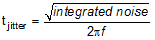
Phase noise is defined by the ratio of noise (at an offset frequency from the oscillating signal, with a 1-Hz bandwidth) to the signal amplitude of the oscillating signal. Integrated noise is essentially the sum of all the phase noise within a defined range of offset frequencies from the oscillating signal (see Figure 2-2). Jitter is derived from Equation 2 using the integrated noise and the frequency of the signal:
The integration range selected is important. This is determined by the sampling settings of the ADC. The bottom range (closer to the oscillating signal) is defined by half of [sampling rate] / [FFT size]. For example, at a sample rate of 2949.12 MHz and FFT size of 65536, the integration goes down to 22.5 kHz (see SLYT379 for more information). Thus, the lower this bottom of the integration range, the more the phase noise at lower offsets matter.
 Figure 2-2 Phase Noise and Jitter Definitions
3 Designing for Lowest Jitter
Now we focus on how to get the lowest possible jitter on the ADC clock source. Figure 3-1 shows a phase noise plot with output frequency at 2949.12 MHz. The black line is the closed loop (locked) phase noise and the red is the open loop (free running VCO) phase noise. Also, the PLL noise is modeled by a flicker noise component (gray line) and a flat PLL noise floor component (blue line). The sum of the two lines is the PLL noise. The loop bandwidth (where the phase noise starts to roll off) is around 100-kHz offset. If this loop bandwidth is low, the VCO noise pushes into the lower offset phase noise, and if the loop bandwidth is high, it can push the PLL phase noise into the VCO region. Generally, to design a loop filter for the lowest jitter, the point where the PLL noise model intersects the VCO is the optimal point (around 120 kHz in this example). This loop bandwidth is determined by the loop filter components of a clocking source, or in this case, an RF synthesizer (integrated PLL + VCO).
 Figure 3-1 Sampling Clock of 2949.12 MHz With 58 fs Jitter