AVB (Audio Video Bridging) protocols have been widely adopted to achieve time and clock synchronization over Ethernet, especially in automotive infotainment systems. CDCE6214-Q1 is a compact and ultra low-power programmable clock generator that supports output frequency tuning with less than 1-ppm step size. With the frequency margining capability, CDCE6214-Q1 is ideal for AVB media clock synchronization. This application report introduces AVB system architecture and explains media clock synchronization design with CDCE6214-Q1.
Texas Instruments, is a registered trademark of Texas Instruments.
AVnu Alliance, AVnu are registered trademarks of AVnu Alliance, Inc.
XMOS, is a registered trademark of Acorn Technologies, Inc.
Harman is a registered trademark of Harman International Industries, Inc.
All other trademarks are the property of their respective owners.
Modern media systems for automotive infotainment and driver assistance are composed of multiple sensors, cameras, displayes, and content players. Point-to-point interconnections with shielded twisted pair or coaxial cables may not be practical for all of the required components. Ethernet is gaining more traction in the automotive audio visual market segment due to its convenience and fast transmission speed; however, standard asynchronous Ethernet networks do not carry clock synchronization information. One of the main goals of AVB protocols is to achieve time and clock synchronization over Ethernet.
Consider the example below where the live or playback audio and video are presented on two RSE (Rear Seat Entertainment) displays and multiple speakers at the same time. Speakers and RSE displays are connected to the Head Unit through Ethernet. For excellent user experience, media content should be lip synchronized, and both audio and video should be distributed to all speakers and displays synchronously.
Two types of A/V synchronization are required:
See Section 2, Section 3 and Section 4 to understand how to achieve the two types of synchronization and how the CDCE6214-Q1 device fits in media clock recovery.
AVB is a family of protocols that include:
An example AVB system is shown in Figure 2:
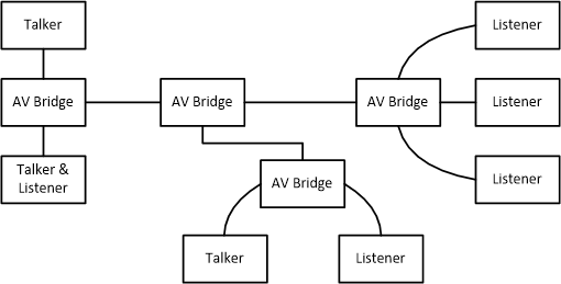
An AVB network consists of three types of components:
To understand more about the AVB end stations see Section 3.
A high level system block diagram of an AVB end station (Talker and Listener) with time-sensitive applications is shown below:
An AVB end station consists of the following components:
Details of media clock recovery and synchronization are covered in the next section.
In this section, the following questions are answered:
A simplified Talker block diagram is shown below:
This diagram explains how the media clock source is embedded into AVTP packets. The media clock's source can be a simple free-running local oscillator, because the media clock does not need to lock to any reference, as long as the frequency of all media clocks in the same domain are synchronized. The media clock goes into a local timestamp generator that generates timestamps every certain number of media clock rising edges. These timestamps are generated based off of a local time reference. The Wall Clock then translates the local time based timestamps to gPTP timestamps. The AVTP Talker adds a fixed offset (typically the maximum delay between the Talker and all Listeners) and generates presentation timestamps.
The AVTP Presentation Time represents the gPTP time at which a designated media sample or event is transferred to the time-sensitive application within each Listener. This enables multiple Listeners to present data at the same time, regardless of the location of the Listeners in the network. The AVTP Presentation Time tells a Listener when to start processing the stream's data (for example, playing media) and is also used to recover the stream's media clock. To understand how to use Presentation time to recover the stream's media clock see Section 4.2.
A simplified Listener block diagram is shown below:
This diagram explains how a Listener extracts presentation timestamps and recovers the source media clock from incoming 1722 streams generated by a Talker. The period of the source media clock in the gPTP time base can be estimated by the time difference between two presentation timestamps divided by the number of samples in between. Continually performing this calculation and applying appropriate filtering techniques yields an accurate measurement of the source's media clock period.
Similarly, the local media clock generator (CDCE6214-Q1) output can be timestamped with local time base which is then translated to gPTP time base, and its period can also be accurately measured. After comparing the two clock periods, the Media Clock Recovery module continually generates I2C/GPIO commands to increment or decrement output frequency of the CDCE6214-Q1 device so that the local media clock is synchronized to the source media clock.
A simplified CDCE6214-Q1 schematic is shown below:
CDCE6214-Q1 has integrated crystal driver circuit, so only a simple crystal resonator is needed at the input. The XTAL (crystal) selection and programming guide can be found at CDCE6214-Q1 Crystal-Based Oscillator Design. The media clock can be generated out of OUT1_P. OUT0 bypasses PLL and produces buffered output from the crystal input. This 25-MHz output can be used to clock Ethernet. The frequency increment and decrement commands coming from media clock recovery module is fed back to the CDCE6214-Q1 device through the I2C (it can also be fed through the GPIO pin control)
The frequency increment and decrement step size can be set by register R43[15:0] FREQ_INC_DEC_DELTA. The VCO (Voltage Controlled Oscillator) frequency step size is PFD_FREQ / PLL_DEN × FREQ_INC_DEC_DELTA, where PFD_FREQ is phase frequency detector frequency and PLL_DEN is the denominator of PLL fractional divider. The output frequency step size is VCO frequency step size divided by output divider. An example calculation can be found in Table 1. Alternatively, the calculation can be done in TicsPro.
PARAMETERS | VALUE (EXAMPLE) | DESCRIPTION |
---|---|---|
Input PFD Frequency (FPFD) | 25 MHz | Set according to FPFD. |
Expected VCO Frequency (FVCO) | 2457.6 MHz | FVCO is set within the operating VCO range of 2335 MHz - 2625 MHz. FVCO is selected such that PSA/PSB/Output Divider is Integer. |
Expected Output Frequency (FOUT) | 24.576 MHz | PSA = 4, IOD = 25. FVCO = PSA × IOD × FOUT. |
Expected step size (in ppm) (Fstep) | 0.1 | Every rising edge of FREQ_INC/FREQ_DEC would change the output by this step size. |
N-divider Value (N) | 98 | INT(FVCO/FPFD) |
Minimum Numerator value to meet 0ppb accuracy (Num) | 76 | These values are computed to meet accuracy requirement at output. Should be less than 224. |
Minimum Denominator to meet 0ppb accuracy (Den) | 250 | |
Minimum Denominator value to meet ppm step size (FDEN,min) | 101725.26 | 1/(Fstep × 1e6) / (FVCO/FPFD) |
Final Denominator value (FDEN,final) | 500000 | FDEN,final should be greater than FDEN,min and less than 224. FDEN,final and FNUM,final should be integer multiple of Den and Num respectively. FDEN,final/Den = FNUM,final/Num |
Final Numerator value (FNUM,final) | 152000 | |
Increment/ Decrement step size | 5 | This value should be less than 216-1. FDEN,final should be closest integer multiple of FDEN,min. |
Once the step size is set, DCO mode is enabled (R3[3] FREQ_INC_DEC_EN = 1) and DCO register control is enabled (R3[4] FREQ_INC_DEC_REG_MODE = 1), the frequency can be incremented or decremented by toggling R3[5] FREQ_INC_REG and R3[6] FREQ_DEC_REG
This application note answers the two frequently asked questions on AVB synchronization:
As described in Section 5, CDCE6214-Q1 is a simple but efficient frequency adjustable PLL that can be used for media clock generation and synchronization. Besides, CDCE6214-Q1 has less than 2.1 ps integrated fractional jitter. It also provides features such as output slew rate control that can slow down the output edge rate and meet EMI requirements for the automotive industry.
TI PROVIDES TECHNICAL AND RELIABILITY DATA (INCLUDING DATASHEETS), DESIGN RESOURCES (INCLUDING REFERENCE DESIGNS), APPLICATION OR OTHER DESIGN ADVICE, WEB TOOLS, SAFETY INFORMATION, AND OTHER RESOURCES “AS IS” AND WITH ALL FAULTS, AND DISCLAIMS ALL WARRANTIES, EXPRESS AND IMPLIED, INCLUDING WITHOUT LIMITATION ANY IMPLIED WARRANTIES OF MERCHANTABILITY, FITNESS FOR A PARTICULAR PURPOSE OR NON-INFRINGEMENT OF THIRD PARTY INTELLECTUAL PROPERTY RIGHTS. |
These resources are intended for skilled developers designing with TI products. You are solely responsible for (1) selecting the appropriate TI products for your application, (2) designing, validating and testing your application, and (3) ensuring your application meets applicable standards, and any other safety, security, or other requirements. These resources are subject to change without notice. TI grants you permission to use these resources only for development of an application that uses the TI products described in the resource. Other reproduction and display of these resources is prohibited. No license is granted to any other TI intellectual property right or to any third party intellectual property right. TI disclaims responsibility for, and you will fully indemnify TI and its representatives against, any claims, damages, costs, losses, and liabilities arising out of your use of these resources. |
TI’s products are provided subject to TI’s Terms of Sale (www.ti.com/legal/termsofsale.html) or other applicable terms available either on ti.com or provided in conjunction with such TI products. TI’s provision of these resources does not expand or otherwise alter TI’s applicable warranties or warranty disclaimers for TI products. |
Mailing Address: Texas Instruments, Post Office Box 655303, Dallas, Texas 75265
Copyright © 2020, Texas Instruments Incorporated |