-
CDCI6214 Ultra-Low Power Clock Generator With PCIe Support, Four Programmable Outputs and EEPROM
- 1
- 1 Features
- 2 Applications
- 3 Description
- 4 Device Comparison
- 5 Pin Configuration and Functions
-
6 Specifications
- 6.1 Absolute Maximum Ratings
- 6.2 ESD Ratings
- 6.3 Recommended Operating Conditions
- 6.4 Thermal Information
- 6.5 EEPROM Characteristics
- 6.6 Reference Input, Single-Ended and Differential Mode Characteristics (REFP, REFN, FB_P, FB_N)
- 6.7 Reference Input, Crystal Mode Characteristics (XIN, XOUT)
- 6.8 General-Purpose Input and Output Characteristics (GPIO[4:1], SYNC/RESETN)
- 6.9 Triple Level Input Characteristics (EEPROMSEL, REFSEL)
- 6.10 Reference Mux Characteristics
- 6.11 Phase-Locked Loop Characteristics
- 6.12 Closed-Loop Output Jitter Characteristics
- 6.13 Output Mux Characteristics
- 6.14 LVCMOS Output Characteristics
- 6.15 HCSL Output Characteristics
- 6.16 LVDS DC-Coupled Output Characteristics
- 6.17 Programmable Differential AC-Coupled Output Characteristics
- 6.18 Output Skew and Delay Characteristics
- 6.19 Output Synchronization Characteristics
- 6.20 Timing Characteristics
- 6.21 I2C-Compatible Serial Interface Characteristics (SDA/GPIO2, SCL/GPIO3)
- 6.22 Timing Requirements, I2C-Compatible Serial Interface (SDA/GPIO2, SCL/GPIO3)
- 6.23 Power Supply Characteristics
- 6.24 Typical Characteristics
- 7 Parameter Measurement Information
-
8 Detailed Description
- 8.1 Overview
- 8.2 Functional Block Diagram
- 8.3 Feature Description
- 8.4 Device Functional Modes
- 8.5 Programming
- 9 Application and Implementation
- 10Register Maps
- 11Device and Documentation Support
- 12Revision History
- 13Mechanical, Packaging, and Orderable Information
- IMPORTANT NOTICE
CDCI6214 Ultra-Low Power Clock Generator With PCIe Support, Four Programmable Outputs and EEPROM
1 Features
- One configurable high performance, low-power PLL with four programmable outputs
- RMS jitter performance
- Supports PCIe Gen1/ Gen2 / Gen3 / Gen4 without SSC
- Typical power consumption: 150mW at 1.8V(2)
- Universal clock input
- Differential AC-coupled or LVCMOS: 1MHz to 250MHz
- Crystal: 8MHz to 50MHz
- Flexible output frequencies
- 44.1kHz to 350MHz
- Glitchless output divider switching
- Four individually configurable outputs
- LVCMOS, LVDS or HCSL
- Differential AC-coupled with programmable swing (LVDS-, CML-, LVPECL-compatible)
- Fully integrated PLL, configurable loop bandwidth: 100kHz to 3MHz
- Single or mixed supply operation for level translation: 1.8V, 2.5V and 3.3V
- Configurable GPIOs
- Status signals
- Up to four individual output enables
- Output divider synchronization
- Flexible configuration options
- I2C-compatible interface: up to 400kHz
- Integrated EEPROM with two pages and external select pin
- Only supports 100Ω systems
- Industrial temperature range: –40°C to 85°C
- Small footprint: 24-pin VQFN (4mm × 4mm)
2 Applications
- PCIe Gen 1/2/3/4 clocking
- 1G / 10G Ethernet switches, NIC, accelerators
- Test & measurement, handheld equipment
- Multi-function printers
- Broadcast infrastructure
3 Description
The CDCI6214 device is an ultra-low power clock generator. The device selects between two independent reference inputs to a phase-locked loop and generates up to four different frequencies on configurable differential output channels and also a copy of the reference clock on a LVCMOS output channel.
Each of the four output channels has a configurable integer divider. Together with the output muxes, this allows up to five different frequencies. Clock distribution dividers are reset in a deterministic way for clean clock gating and glitch-less update capability. Flexible power-down options allow to optimize the device for lowest power consumption in active and standby operation. Typically four 156.25MHz LVDS outputs consume 150mW at 1.8V. Typical RMS jitter of 386fs for 100MHz HCSL output enhances system margin for PCIe applications.
The CDCI6214 is configured using internal registers that are accessed by an I2C-compatible serial interface and internal EEPROM.
The CDCI6214 enables high-performance clock trees from a single reference at ultra-low power with a small footprint. The factory- and user-programmable EEPROM of the CDCI6214 is designed as an easy-to-use, instant-on clocking feature with low power consumption.
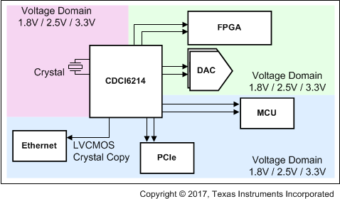
 Application Example CDCI6214