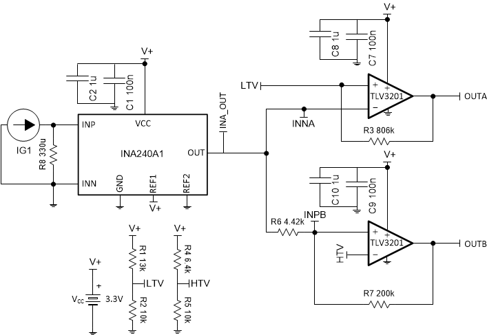
Bidirectional Current Sensing with a Window Comparator Circuit
Design Goals
| SYSTEM CURRENT LEVELS | SUPPLY | ||||
|---|---|---|---|---|---|
| Falling OC Threshold | Falling OC Recovery | Rising OC Threshold | Rising OC Recovery | V+ | V- |
| IG1 < -35A | IG1 > -31A | IG1 > 100A | IG1 < 90A | 3.3V | 0V |
Design Description
This bidirectional current sensing solution uses a current-sense amplifier and a high speed dual comparator with a rail-to-rail input common mode range to create over-current (OC) alert signals at the comparator outputs (OUTA and OUTB) if the input current (IG1) rises above 100A or falls below -35A. In this implementation, both over-current alert signals are active high, so when the 100A or -35A thresholds are crossed, the comparator outputs goes high. External hysteresis is implemented on both comparators so that the comparator outputs return to logic low states when the current reduces by 10% (90A and -31A). While the circuit below has shunt resistor R8 connected to ground, the same circuit is applicable for high side current sensing up to the common mode voltage range of the INA.
Design Notes
- Select a comparator with rail-to-rail input common mode range.
- Select a current sense amplifier with low offset voltage and a common mode input range that matches the requirements of the system.
Design Steps
- To determine
the comparator threshold voltages, first calculate the INA240A1 output voltages
that correspond to the desired current thresholds. The calculations depend on
the gain of the INA240 (20, 50, 100, 200 for A1, A2, A3, A4, respectively), the
input current (IG1) and sense resistor (R8), and the reference voltage when the
input current is 0 (VREF). Per section 8.3.2 in the INA240 data sheet, R8 is a
function of the differential input voltage and the maximum input current to the
INA240. Given that the input current in this system swings above 100A, by
keeping R8 small, the power dissipation across R8 is lessened.
Using these equations and the desired current thresholds, the following table is generated:DESCRIPTION IG1 INA-OUT VH, CHB Overcurrent threshold in forward direction 100A 1.65V + 20 × (100A × 0.33mΩ) = 2.31V VL, CHB Recovery threshold in forward direction 90A 1.65V + 20 × (90A × 0.33mΩ) = 2.244V VH, CHA Overcurrent threshold in reverse direction -35A 1.65V + 20 × (-35A × 0.33mΩ) = 1.419V VL, CHA Recovery threshold in reverse direction -31.5A 1.65V + 20 × (-31.5A × 0.33mΩ) = 1.4421V First, focus on the top comparator (channel A), which is in an inverting comparator configuration. This comparator swings to a logic high when the current in the reverse direction exceeds -35A, and returns to a logic low when the current in the reverse direction recovers to -31.5A. These current levels correspond to voltage levels of 1.419V and 1.4421V, respectively.
- Assume a value for R2 (the bottom resistor in the resistor divider). In this circuit, 10kΩ is chosen.
- Derive two equations for R1 in
terms of V+, VL, VH, R2, R3 by
analyzing the circuit when INNA = VL and when INNA = VH:
- Set these two equations equal to
each other and then solve for R3.
The standard 1% resistor value closest to this is 806kΩ.
- Solve for
R1 using any of the two equations derived in 3:
The standard 1% resistor value closest to this is 13kΩ.
The next step is to focus on the bottom comparator (channel B), which is in a non-inverting configuration. This comparator swings to a logic high when the current in the forward direction exceeds 100A, and returns to a logic low when the current in the forward direction recovers to 90A. These current levels correspond to voltage levels of 2.31V and 2.244V, respectively.
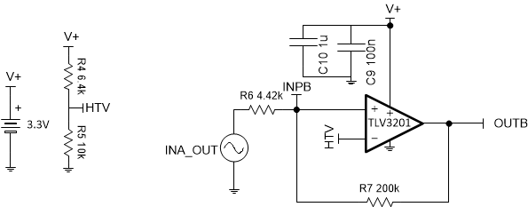
High-side current sensing with comparator circuit derives two equations for VTH (the voltage on the non-inverting pin) when the comparator output is in a logic low state and a high-impedance state (SBOA306 uses an open-drain comparator). These equations are then set equal to each other creating a quadratic equation to solve for R6. Since TLV3202 is a push-pull device, the output goes to a logic high state instead of a high-impedance state. Thus, the pull-up resistor value is 0 and VPU is V+
- Rewrite the quadratic equation to
match this circuit:
- Choose a value for R7.
This resistor dictates the load current of the comparator, and therefore is
large. For this circuit, R7 is assumed to be 200kΩ.
The standard 1% resistor value closest to this is 4.42kΩ.
- Calculate VTH using
R6.
- Choose a value for R5.
In this case, R5 is chosen to be 10kΩ.
- Solve for
R4.
The standard 1% resistor value closest to this is 4.64kΩ.
Design Simulations
Transient Simulation Results
The below simulation results use a -70A to 130A, 100Hz sine wave for IG1.
 Channel A
 Channel B
Design References
Texas Instruments, SBOMB05 SPICE file, circuit software
Design Featured Comparator
| TLV320x | |
|---|---|
| VS | 2.7V to 5.5V |
| VinCM | 200mV beyond either rail |
| VOUT | Push-Pull, Rail-to-rail |
| VOS | 1mV |
| IQ | 40µA/channel |
| tPD(HL) | 40ns |
| #Channels | 1, 2 |
| TLV3201-Q1 and TLV3202-Q1 | |
Design Featured Op Amp
| INA240 | |
|---|---|
| VS | 1.6V to 5.5V |
| VinCM | -4V to 80V |
| VOUT | Rail-to-rail |
| VOS | 5µV |
| VOS Drift | 50nV/◦C |
| IQ | 260ns |
| Gain Options | 20V/V, 50V/V, 100V/V, 200V/V |
| INA240 | |
Trademarks
All trademarks are the property of their respective owners.
IMPORTANT NOTICE AND DISCLAIMER
TI PROVIDES TECHNICAL AND RELIABILITY DATA (INCLUDING DATASHEETS), DESIGN RESOURCES (INCLUDING REFERENCE DESIGNS), APPLICATION OR OTHER DESIGN ADVICE, WEB TOOLS, SAFETY INFORMATION, AND OTHER RESOURCES “AS IS” AND WITH ALL FAULTS, AND DISCLAIMS ALL WARRANTIES, EXPRESS AND IMPLIED, INCLUDING WITHOUT LIMITATION ANY IMPLIED WARRANTIES OF MERCHANTABILITY, FITNESS FOR A PARTICULAR PURPOSE OR NON-INFRINGEMENT OF THIRD PARTY INTELLECTUAL PROPERTY RIGHTS.
These resources are intended for skilled developers designing with TI products. You are solely responsible for (1) selecting the appropriate TI products for your application, (2) designing, validating and testing your application, and (3) ensuring your application meets applicable standards, and any other safety, security, or other requirements. These resources are subject to change without notice. TI grants you permission to use these resources only for development of an application that uses the TI products described in the resource. Other reproduction and display of these resources is prohibited. No license is granted to any other TI intellectual property right or to any third party intellectual property right. TI disclaims responsibility for, and you will fully indemnify TI and its representatives against, any claims, damages, costs, losses, and liabilities arising out of your use of these resources.
TI’s products are provided subject to TI’s Terms of Sale (www.ti.com/legal/termsofsale.html) or other applicable terms available either on ti.com or provided in conjunction with such TI products. TI’s provision of these resources does not expand or otherwise alter TI’s applicable warranties or warranty disclaimers for TI products.
Mailing Address: Texas Instruments, Post Office Box 655303, Dallas, Texas 75265
Copyright © 2024, Texas Instruments Incorporated