SNVA920B January 2020 – September 2021 LM61430-Q1 , LM61435-Q1 , LM61440-Q1 , LM61460-Q1
This document contains information for LM61430-Q1, LM61435-Q1, LM61440-Q1, and LM61460-Q1 (VQFN-HR package) to aid in a functional safety system design. Information provided are:
Figure 1-1 shows the device functional block diagram for reference.
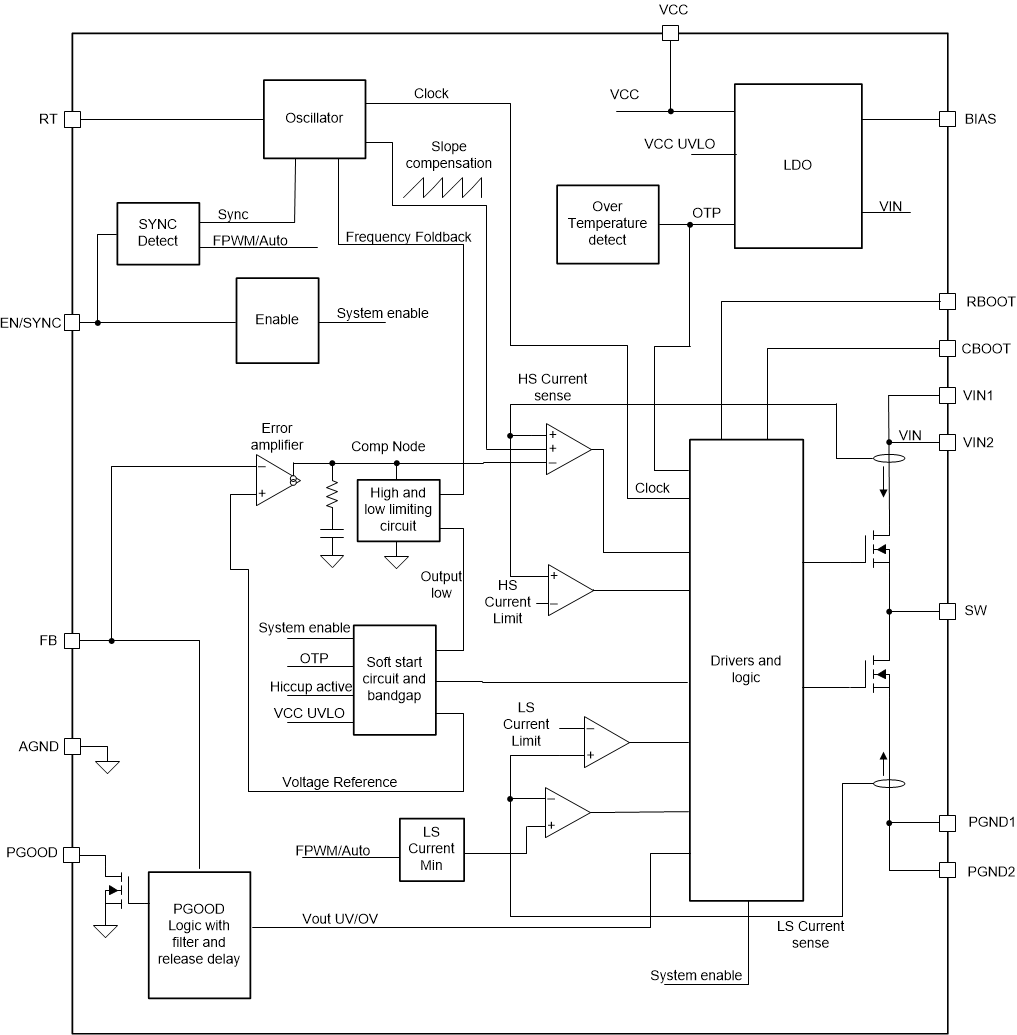
LM61430-Q1, LM61435-Q1, LM61440-Q1, and LM61460-Q1 was developed using a quality-managed development process, but was not developed in accordance with the IEC 61508 or ISO 26262 standards.
This section provides Functional Safety Failure In Time (FIT) rates for LM61430-Q1, LM61435-Q1, LM61440-Q1, and LM61460-Q1 based on two different industry-wide used reliability standards:
FIT IEC TR 62380 / ISO 26262 | FIT (Failures Per 109 Hours) |
---|---|
Total Component FIT Rate | 17 |
Die FIT Rate | 9 |
Package FIT Rate | 8 |
The failure rate and mission profile information in Table 2-1 comes from the Reliability data handbook IEC TR 62380 / ISO 26262 part 11:
Table | Category | Reference FIT Rate | Reference Virtual TJ |
---|---|---|---|
5 | CMOS, BiPolar | 25 FIT | 55°C |
The Reference FIT Rate and Reference Virtual TJ (junction temperature) in Table 2-2 come from the Siemens Norm SN 29500-2 tables 1 through 5. Failure rates under operating conditions are calculated from the reference failure rate and virtual junction temperature using conversion information in SN 29500-2 section 4.
The failure mode distribution estimation for LM61430-Q1, LM61435-Q1, LM61440-Q1, and LM61460-Q1 in Table 3-1 comes from the combination of common failure modes listed in standards such as IEC 61508 and ISO 26262, the ratio of sub-circuit function size and complexity and from best engineering judgment.
The failure modes listed in this section reflect random failure events and do not include failures due to misuse or overstress.
Die Failure Modes | Failure Mode Distribution (%) |
---|---|
SW No output | 45% |
SW output not in specification - voltage or timing | 40% |
SW power FET stuck on | 5% |
PGOOD false trip, fails to trip | 5% |
Short circuit any two pins | 5% |
The FMD in Table 3-1 excludes short circuit faults across the isolation barrier. Faults for short circuit across the isolation barrier can be excluded according to ISO 61800-5-2:2016 if the following requirements are fulfilled:
Creepage and clearance requirements should be applied according to the specific equipment isolation standards of an application. Care should be taken to maintain the creepage and clearance distance of a board design to ensure that the mounting pads of the isolator on the printed-circuit board do not reduce this distance.
This section provides a Failure Mode Analysis (FMA) for the pins of the LM61430-Q1, LM61435-Q1, LM61440-Q1, and LM61460-Q1. The failure modes covered in this document include the typical pin-by-pin failure scenarios:
Table 4-2 through Table 4-5 also indicate how these pin conditions can affect the device as per the failure effects classification in Table 4-1.
Class | Failure Effects |
---|---|
A | Potential device damage that affects functionality |
B | No device damage, but loss of functionality |
C | No device damage, but performance degradation |
D | No device damage, no impact to functionality or performance |
Figure 4-1 shows the LM61430-Q1, LM61435-Q1, LM61440-Q1, and LM61460-Q1 pin diagram. For a detailed description of the device pins please refer to the 'Pin Configuration and Functions' section in the LM61430-Q1, LM61435-Q1, LM61440-Q1, and LM61460-Q1 datasheet.
Following are the assumptions of use and the device configuration assumed for the pin FMA in this section:
Pin Name | Pin No | Description of Potential Failure Effect(s) | Failure Effect Class |
---|---|---|---|
BIAS | 1 | Normal operation | D |
VCC | 2 | VOUT = 0 V | B |
AGND | 3 | Normal operation | D |
FB | 4 | VOUT >> than the programmed output voltage. | B |
PGOOD | 5 | PGOOD is not a valid signal. VOUT is in regulation. | D |
RT | 6 | VOUT = 0 V | B |
EN/SYNC | 7 | VOUT = 0 V | B |
VIN1 | 8 | VOUT = 0 V | B |
PGND1 | 9 | VOUT is normal. | D |
SW | 10 | Damage to HS FET | A |
PGND2 | 11 | VOUT is normal. | D |
VIN2 | 12 | VOUT = 0 V | B |
RBOOT | 13 | VOUT = 0 V | A |
CBOOT | 14 | VOUT = 0 V | B |
Pin Name | Pin No | Description of Potential Failure Effect(s) | Failure Effect Class |
---|---|---|---|
BIAS | 1 | Normal operation | D |
VCC | 2 | VCC output will be unstable and can increase above 5.5-V rating of the VCC pin. | A |
AGND | 3 | VOUT can be abnormal due to switching noise on analog circuits. | B |
FB | 4 | VOUT >> than the programmed output voltage. | B |
PGOOD | 5 | PGOOD is not a valid signal. VOUT is in regulation. | D |
RT | 6 | VOUT = 0 V | B |
EN/SYNC | 7 | Unpredictable operation | B |
VIN1 | 8 | VOUT is normal. Current loop will be affected, potentially affecting noise/jitter/EMI/reliability. | C |
PGND1 | 9 | VOUT is normal. Current loop will be affected, potentially affecting noise/jitter/EMI/reliability. | C |
SW | 10 | VOUT = 0 V | B |
PGND2 | 11 | VOUT is normal. All current will be in this loop, potentially affecting noise/jitter/EMI/reliability. | C |
VIN2 | 12 | VOUT is normal. All current will be in this loop, potentially affecting noise/jitter/EMI/reliability. | C |
RBOOT | 13 | VOUT normal | D |
CBOOT | 14 | VOUT = 0 V | B |
Pin Name | Pin No | Description of Potential Failure Effect(s) | Failure Effect Class |
---|---|---|---|
BIAS | 1 | VCC ESD clamp damaged if BIAS > 5 V. | A |
VCC | 2 | VOUT = 0 V | B |
AGND | 3 | VOUT >> than programmed output voltage. | B |
FB | 4 | VOUT = 0 V, Damage if PGOOD > 16 V. | A |
PGOOD | 5 | VOUT = 0 V | B |
RT | 6 | VOUT = 0 V, Damage if EN/SYNC > 5.5 V. | A |
EN/SYNC | 7 | VOUT normal | D |
VIN1 | 8 | VOUT = 0 V | B |
PGND1 | 9 | VOUT = 0 V. Damage to low-side circuitry if PGND >> AGND | B |
SW | 10 | Damage to HS FET | A |
PGND2 | 11 | VOUT = 0 V. Damage to low-side circuitry if PGND >> AGND | B |
VIN2 | 12 | VOUT = 0 V | B |
RBOOT | 13 | VOUT normal | D |
CBOOT | 14 | VOUT = 0 V | B |
Pin Name | Pin No | Description of Potential Failure Effect(s) | Failure Effect Class |
---|---|---|---|
BIAS | 1 | If VIN exceeds 16 V, damage will occur. If below, normal operation | A |
VCC | 2 | If VIN exceeds 5.5 V, damage will occur. | A |
AGND | 3 | VOUT = 0 V. Damage to other pins referred to GND. | A |
FB | 4 | If VIN exceeds 16 V, damage will occur. VOUT = 0 V. | A |
PGOOD | 5 | VOUT = 0 V. PGOOD ESD clamp will run current to destruction. | A |
RT | 6 | VOUT = 0 V | B |
EN/SYNC | 7 | VOUT normal | D |
VIN1 | 8 | Normal operation | D |
PGND1 | 9 | VOUT = 0 V. Damage to low-side circuitry if PGND >> AGND | B |
SW | 10 | Damage to LS FET | A |
PGND2 | 11 | VOUT = 0 V. Damage to low-side circuitry if PGND >> AGND | B |
VIN2 | 12 | Normal operation | D |
RBOOT | 13 | VOUT = 0 V. RBOOT ESD clamp will run current to destruction. | A |
CBOOT | 14 | VOUT = 0 V. CBOOT ESD clamp will run current to destruction. | A |