-
TPS9264x Synchronous Buck Controllers for Precision Dimming LED Drivers
- 1 Features
- 2 Applications
- 3 Description
- 4 Revision History
- 5 Pin Configuration and Functions
- 6 Specifications
-
7 Detailed Description
- 7.1 Overview
- 7.2 Functional Block Diagram
- 7.3
Feature Description
- 7.3.1 Controlled On-Time Architecture
- 7.3.2 Switching Frequency
- 7.3.3 Average LED Current
- 7.3.4 Analog Dimming and True-Zero Operation
- 7.3.5 Undervoltage Lockout (UVLO)
- 7.3.6 PWM Dimming Using the UDIM Pin
- 7.3.7 External Shunt FET PWM Dimming
- 7.3.8 VCC Regulation and Start-up
- 7.3.9 Precision Reference
- 7.3.10 Control Loop Compensation
- 7.3.11 Overcurrent Protection
- 7.3.12 Overvoltage Protection (OVP)
- 7.3.13 Boot Undervoltage Lockout (UVLO)
- 7.4 Device Functional Modes
-
8 Application and Implementation
- 8.1 Application Information
- 8.2
Typical Applications
- 8.2.1
TPS92640: Design Procedure
- 8.2.1.1 Design Requirements
- 8.2.1.2
Detailed Design Procedure
- 8.2.1.2.1 Set Output Voltage Feedback Ratio
- 8.2.1.2.2 Set Switching Frequency
- 8.2.1.2.3 Set Average LED Current
- 8.2.1.2.4 Set Inductor Ripple Current
- 8.2.1.2.5 Set LED Ripple Current and Determine Output Capacitance, COUT
- 8.2.1.2.6 Choose N-Channel MOSFETs
- 8.2.1.2.7 Choose Input Capacitance
- 8.2.1.2.8 Set the Turnon Voltage and Undervoltage Lockout Hysteresis
- 8.2.2
TPS92640 - PWM Dimming Application
- 8.2.2.1 Design Requirements
- 8.2.2.2
Detailed Design Procedure
- 8.2.2.2.1 Calculate Operating Points
- 8.2.2.2.2 Output Voltage Feedback
- 8.2.2.2.3 Switching Frequency
- 8.2.2.2.4 Set the Feedback Reference and LED Current
- 8.2.2.2.5 Calculate the Inductor Value
- 8.2.2.2.6 Calculate the Output Capacitor Value
- 8.2.2.2.7 Calculate the MOSFET Parameters
- 8.2.2.2.8 Calculate the Minimum Input Capacitance
- 8.2.2.2.9 Undervoltage Lockout and Hysteresis
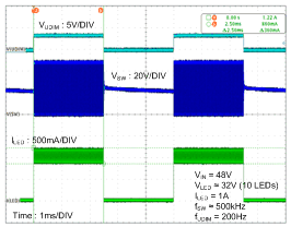
- 8.2.2.3 Application Curve
- 8.2.1
TPS92640: Design Procedure
- 9 Power Supply Recommendations
- 10Layout
- 11Device and Documentation Support
- 12Mechanical, Packaging, and Orderable Information
- IMPORTANT NOTICE
TPS9264x Synchronous Buck Controllers for Precision Dimming LED Drivers
1 Features
- VIN Range from 7 V to 85 V
- Wide Dimming Range
- 500:1 Analog Dimming
- 2500:1 Standard PWM Dimming
- 20000:1 Shunt FET PWM Dimming
- Adjustable LED Current Sense Voltage
- 2-Ω, 1-Apeak MOSFET Gate Drivers
- Shunt Dimming MOSFET Gate Driver (TPS92641)
- Programmable Switching Frequency
- Precision Voltage Reference 3 V ±2%
- Input UVLO and Output OVP
- Low Power Shutdown Mode and Thermal Shutdown
2 Applications
- LED Driver / Constant Current Regulator
- Architectural LED Lighting Drivers
- Automotive LED Drivers
- General LED Illumination
3 Description
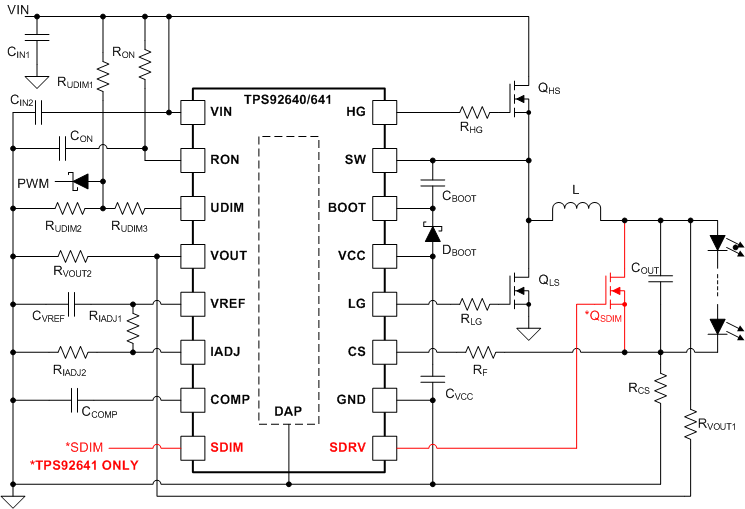
The TPS92640 and TPS92641 devices are high-voltage, synchronous NFET controllers for buck-current regulators. Output current regulation is based on valley current-mode operation using a controlled on-time architecture. This control method eases the design of loop compensation while maintaining nearly constant switching frequency. The TPS92640 and TPS92641 devices include a high-voltage start-up regulator that operates over a wide input range of 7 V to 85 V. The PWM controller is designed for high speed capability, including an oscillator frequency range up to 1 MHz. The deadtime between high side and low side gate driver is optimized to provide very high efficiency over a wide input operating voltage and output power range. The TPS92640 and TPS92641 devices accept both analog and PWM input signals, resulting in exceptional dimming control range. Linear response characteristics between input command and LED current is achieved with true zero LED current using low off-set error amplifier and proprietary PWM dimming logic. Both devices also include precision reference capable of supplying current to low power microcontroller. Protection features include cycle-by-cycle current protection, overvoltage protection, and thermal shutdown. The TPS92641 device includes a shunt FET dimming input and MOSFET driver for high resolution PWM dimming.
Device Information(1)
| PART NUMBER | PACKAGE | BODY SIZE (NOM) |
|---|---|---|
| TPS92640 | HTSSOP (14) | 4.40 mm × 5.00 mm |
| TPS92641 | HTSSOP (16) | 4.40 mm × 5.00 mm |
- For all available packages, see the orderable addendum at the end of the data sheet.
Typical Application Diagram
4 Revision History
Changes from * Revision (October 2012) to A Revision
- Added ESD Ratings table, Feature Description section, Device Functional Modes, Application and Implementation section, Power Supply Recommendations section, Layout section, Device and Documentation Support section, and Mechanical, Packaging, and Orderable Information section. Go
5 Pin Configuration and Functions


Pin Functions
| PIN | I/O | DESCRIPTION | ||
|---|---|---|---|---|
| NAME | NO. (TPS92640) | NO. (TPS92641) | ||
| BOOT | 12 | 14 | O | Connect 100-nF ceramic capacitor to switch node and diode to VCC to provide boosted voltage for high-side gate drive. |
| COMP | 7 | 7 | O | Connect ceramic capacitor to GND to set loop compensation. |
| CS | 9 | 11 | I | Connect to positive terminal of sense resistor at the bottom of the LED stack. |
| GND | 8 | 10 | — | System GND. Connect to DAP. |
| HG | 14 | 16 | O | Connect to gate of high-side NFET of buck regulator. Use series resistor to limit current slew-rate and mitigate EMI noise. |
| IADJ | 6 | 6 | I | Connect resistor divider from VREF to set analog dimming level. Use NTC resistor from pin to GND as resistor divider to implement thermal foldback operation. |
| LG | 10 | 12 | O | Connect to gate of low-side NFET of buck regulator. Use series resistor to limit current slew-rate and mitigate EMI noise. |
| RON | 2 | 2 | I | Connect a resistor to VIN and capacitor to GND to set switching frequency. |
| SDIM | — | 8 | I | PWM dimming input for shunt FET dimming. |
| SDRV | — | 9 | O | Connect to gate of external parallel NFET across LED load used for shunt dimming if desired. |
| SW | 13 | 15 | O | Connect to switch node of buck regulator. |
| UDIM | 3 | 3 | I | Connect resistor divider from VIN to set undervoltage lockout threshold. |
| VCC | 11 | 13 | O | Bypass with 2.2-µF ceramic capacitor to provide bias supply for controller. |
| VIN | 1 | 1 | I | Connect to input voltage. Connect 1-µF bypass capacitor |
| VOUT | 4 | 4 | I | Connect resistor divider from VOUT, scaled down feedback of VOUT. |
| VREF | 5 | 5 | O | System reference voltage. Bypass with 100-nF ceramic capacitor. |
| DAP | — | — | — | Place 6-9 vias from pad to GND plane for thermal relief. |
6 Specifications
6.1 Absolute Maximum Ratings
over operating free-air temperature range (unless otherwise noted)(1)| MIN | MAX | UNIT | ||
|---|---|---|---|---|
| VIN, UDIM, SW | –0.3 | 90 | V | |
| –1 | mA | |||
| BOOT | –0.3 | 98.5 | V | |
| HG | –0.3 | 90 | V | |
| –2.5 (Pulse < 100 ns) | V | |||
| LG, SDRV, CS | –0.3 | +VCC | V | |
| –2.5 (Pulse < 100 ns) | V | |||
| VCC + 2.5 (Pulse < 100 ns) | V | |||
| VCC | –0.3 | 15 | V | |
| VREF, RON, COMP, VOUT, IADJ, SDIM | –0.3 | 6 | V | |
| –200 | 200 | µA | ||
| GND | –0.3 | 0.3 | V | |
| –2.5 (Pulse < 100 ns) | 2.5 (Pulse < 100 ns) | V | ||
| Continuous power dissipation | Internally Limited | |||
| Maximum lead temperature (soldering and reflow) (2) | 260 | °C | ||
| Maximum junction temperature | –40 | 125 | °C | |
| Storage temperature | –65 | 150 | °C | |
6.2 ESD Ratings
| VALUE | UNIT | |||
|---|---|---|---|---|
| TPS92640 PWP PACKAGE | ||||
| V(ESD) | Electrostatic discharge | Human-body model (HBM), per ANSI/ESDA/JEDEC JS-001(1) | ±2000 | V |
| Charged-device model (CDM), per JEDEC specification JESD22-C101(2) | ±1000 | |||
| TPS92641 PWP PACKAGE | ||||
| V(ESD) | Electrostatic discharge | Human-body model (HBM), per ANSI/ESDA/JEDEC JS-001(1) | ±2000 | V |
| Charged-device model (CDM), per JEDEC specification JESD22-C101(2) | ±1000 | |||
6.3 Recommended Operating Conditions
over operating free-air temperature range (unless otherwise noted)| MIN | NOM | MAX | UNIT | ||
|---|---|---|---|---|---|
| VIN | Input voltage | 7 | 85 | V | |
| TJ | Junction temperature | –40 | 125 | °C | |
6.4 Thermal Information
| THERMAL METRIC(1) | TPS92640 | TPS92641 | UNIT | |
|---|---|---|---|---|
| PWP (HTSSOP) | PWP (HTSSOP) | |||
| 14 PINS | 16 PINS | |||
| RθJA | Junction-to-ambient thermal resistance | 40.1 | 38.7 | °C/W |
| RθJC(top) | Junction-to-case (top) thermal resistance | 24.6 | 22.7 | °C/W |
| RθJB | Junction-to-board thermal resistance | 20.9 | 16.5 | °C/W |
| ψJT | Junction-to-top characterization parameter | 0.6 | 0.6 | °C/W |
| ψJB | Junction-to-board characterization parameter | 20.7 | 16.3 | °C/W |
| RθJC(bot) | Junction-to-case (bottom) thermal resistance | 2.5 | 1.7 | °C/W |
6.5 Electrical Characteristics
Unless otherwise specified VIN = 24 V. Typical specifications apply for TA = TJ = 25°C.| PARAMETER | TEST CONDITIONS | MIN(1) | TYP(2) | MAX(1) | UNIT | |
|---|---|---|---|---|---|---|
| START-UP REGULATOR (VCC, VIN) | ||||||
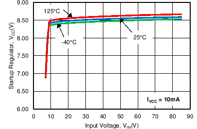
| VCCREG | VCC Regulation | ICC = 10 mA, VIN = 24 V, 85 V | 7.86 | 8.5 | 9.14 | V |
| ICCLIM | VCC Current Limit | VCC = 0 V | 48 | 63 | 78 | mA |
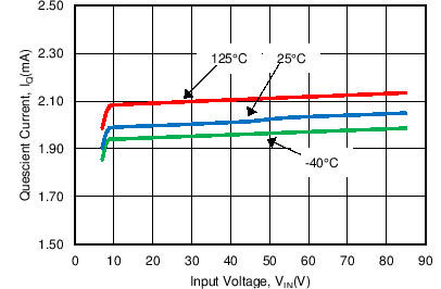
| IQ | Quiescent Current | VUDIM = 3 V, Static VIN = 7 V, 24 V, 85 V |
2 | 3 | mA | |
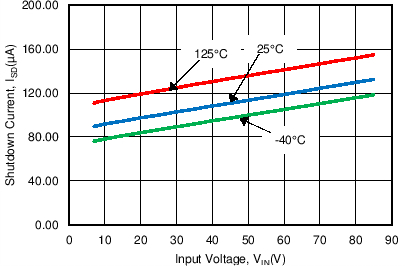
| ISD | Shutdown Current | VUDIM = 0 V | 100 | µA | ||
| VCC-UV | VCC UVLO Threshold | VCC increasing | 5.04 | 5.9 | V | |
| VCC decreasing | 4.5 | 4.9 | ||||
| VCC-HYS | VCC UVLO Hysteresis | 0.17 | V | |||
| REFERENCE VOLTAGE (VREF) | ||||||
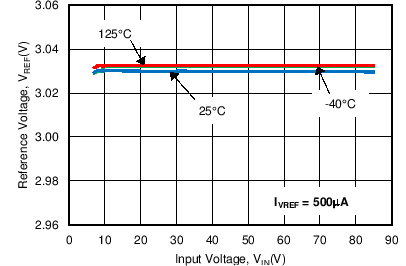
| VREF | Reference Voltage | No Load, VIN = 7 V, 24 V, 85 V | 2.97 | 3.03 | 3.09 | V |
| IVREFLIM | Current Limit | VREF = 0 V | 1.3 | 2.1 | 2.9 | mA |
| ERROR AMPLIFIER (CS, COMP) | ||||||
| VCSREF | CS Reference Voltage | With respect to GND | VIADJ/10 | V | ||
| VCSREF-OFF | Error Amp Input Offset Voltage | –600 | 0 | 600 | µV | |
| ICOMP | COMP Sink Current | 85 | µA | |||
| COMP Source Current | 110 | µA | ||||
| gM-CS | Transconductance | 500 | µA/V | |||
| Linear Input Range | See (3) | ±125 | mV | |||
| Transconductance Bandwidth | –6-dB unloaded response(3) | 400 | kHz | |||
| TIMERS / OVERVOLTAGE PROTECTION (RON, VOUT) | ||||||
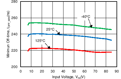
| tOFF-MIN | Minimum Off-time | CS = 0 V | 230 | ns | ||
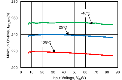
| tON-MIN | Minimum On-time | 235 | ns | |||
| tON | Programmed On-time | VVOUT = 2 V, RON = 25 kΩ, CON = 1 nF | 2.08 | µs | ||
| RRON | RON Pulldown Resistance | 35 | 120 | Ω | ||
| tCL | Current Limit Off-time | 270 | µs | |||
| tD-ON | RON Thresh - HG Falling Delay | 25 | ns | |||
| VTH-OVP | VOUT Overvoltage Threshold | VOUT rising | 2.85 | 3.05 | 3.25 | V |
| VHYS-OVP | VOUT Overvoltage Hysteresis | 0.13 | V | |||
| GATE DRIVER (HG, LG, BOOT, SW) | ||||||
| RSRC-LG | LG Sourcing Resistance | LG = High | 1.5 | 6 | Ω | |
| RSNK-LG | LG Sinking Resistance | LG = Low | 1 | 4.5 | Ω | |
| RSRC-HG | HG Sourcing Resistance | HG = High | 3.9 | 6 | Ω | |
| RSNK-HG | HG Sinking Resistance | HG = Low | 1.1 | 4.5 | Ω | |
| VTH-BOOT | BOOT UVLO Threshold | BOOT-SW rising | 1.9 | 3.4 | 4.5 | V |
| VHYS-BOOT | BOOT UVLO Hysteresis | BOOT-SW falling | 1.8 | V | ||
| TD-HL | HG to LG deadtime | HG fall to LG rise | 60 | ns | ||
| TD-LH | LG to HG deadtime | LG fall to HG rise | 60 | ns | ||
| PWM DIMMING (SDIM, SDRV) (TPS92641 only) | ||||||
| RSRC-DDRV | SDRV Sourcing Resistance | SDRV = High | 5.6 | 30 | Ω | |
| tSDIM-RIS | SDIM to SDRV Rising Delay | SDIM rising | 68 | 100 | ns | |
| tSDIM -FALL | SDIM to SDRV Falling Delay | SDIM falling | 29 | 70 | ns | |
| VSDIM-RIS | SDIM Rising Threshold | SDIM rising | 1.29 | 1.74 | V | |
| VSDIM -FALL | SDIM Falling Threshold | SDIM falling | 0.5 | V | ||
| RSDIM-PU | SDIM Pullup Resistance | 90 | kΩ | |||
| ANALOG ADJUST (IADJ) | ||||||
| VADJ-MAX | IADJ Clamp Voltage | 2.46 | 2.54 | 2.62 | V | |
| RADJ | IADJ Input Impedance | 1 | MΩ | |||
| UNDERVOLTAGE / PWM (UDIM) | ||||||
| VTH-UDIM | UDIM Start-up Threshold | UDIM rising | 1.21 | 1.276 | 1.342 | V |
| IHYS-UDIM | UDIM Hysteresis Current | 12 | 21 | 30 | µA | |
| tUDIM-RIS | UDIM to HG/LG Rising Delay | UDIM rising | 168 | 260 | ns | |
| tUDIM-FALL | UDIM to HG/LG Falling Delay | UDIM falling | 174 | 280 | ns | |
| VUDIM-LP | UDIM Low Power Threshold | 370 | mV | |||
| TUDIM-DET | UDIM Shutdown Detect Timer | UDIM falling | 8.5 | 13 | ms | |
| THERMAL SHUTDOWN | ||||||
| TSD | Thermal Shutdown Threshold | See (3) | 165 | °C | ||
| THYS | Thermal Shutdown Hysteresis | See (3) | 20 | °C | ||
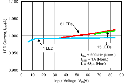
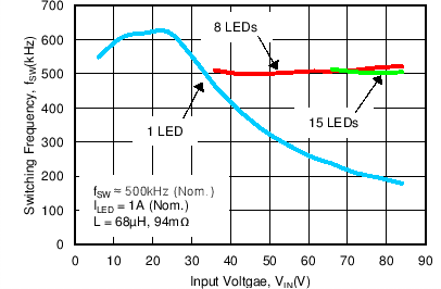
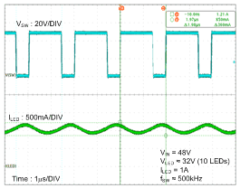
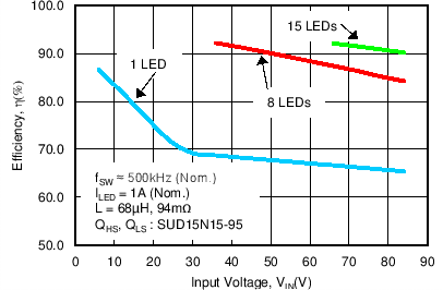
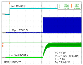
6.6 Typical Characteristics
Unless otherwise stated, –40°C ≤ TA = TJ ≤ 125°C, VIN = 24 V, VIADJ= 2 V, ILED = 1 A, CVCC = 2.2 μF, CCOMP = 0.47 μF