The LM5140-Q1 is a dual synchronous buck controller intended for high voltage wide VIN step-down converter applications. The control method is based on current mode control. Current mode control provides inherent line feedforward, cycle-by-cycle current limiting, and easier loop compensation.
The LM5140-Q1 features adjustable slew rate control to simplify compliance with the CISPR and automotive EMI requirements. The LM5140-Q1 operates at selectable switching frequencies of 2.2 MHz or 440 kHz with the two controller channels switching 180º out of phase. In light or no-load conditions, the LM5140-Q1 operates in skip cycle mode for improved low power efficiency. The LM5140-Q1 includes a high voltage bias regulator with automatic switchover to an external bias supply to improve efficiency and reduce input current. Additional features include frequency synchronization, cycle-by-cycle current limit, hiccup mode fault protection for sustained overloads, independent power good outputs, and independent enable inputs.
PART NUMBER | PACKAGE | BODY SIZE (NOM) |
---|---|---|
LM5140-Q1 | VQFN (40) | 6.00 mm × 6.00 mm |
Changes from * Revision (January 2016) to A Revision
PIN | I/O | DESCRIPTION | |
---|---|---|---|
NO. | NAME | ||
1 | SS2 | I | Channel 2 soft-start programming pin. An external capacitor and an internal 20-μA current source set the ramp rate of the internal error amplifier reference during soft-start. Pulling SS pin below 80 mV turns off the channel 2 gate driver outputs, but all the other functions remain active. |
2 | COMP2 | O | Output of the channel 2 transconductance error amplifier. |
3 | FB2 | I | Feedback input of channel 2. Connect the FB2 pin to VDD for a 5-V output or connect FB2 to ground for a fixed 8-V output. A resistive divider from the VOUT2 to the FB2 pin sets the output voltage level between 1.5 V and 15 V. The regulation threshold at the FB2 pin is 1.2 V. |
4 | CS2 | I | Channel 2 current sense amplifier input. Make a low current Kelvin connection between this pin and the inductor side of the external current sense resistor. |
5 | VOUT2 | I | Output and the current sense amplifier input of channel 2 . Connect this pin to the output side of the channel 2 current sense resistor. |
6 | VCCX | I | Optional input for an external bias supply. If VCCX > 4.5 V, VCCX is internally connected to VCC and the internal VCC regulator is disabled. If VCCX is unused, it must be grounded. |
7 | PG2 | O | An open-collector output which goes low if VOUT2 is outside a specified regulation window. |
8 | HOL2 | O | Channel 2 high-side gate driver turnoff output. |
9 | HO2 | O | Channel 2 high-side gate driver turnon output. |
10 | SW2 | I | Switching node of the channel 2 buck regulator. Connect to the bootstrap capacitor, the source terminal of the high-side MOSFET and the drain terminal of the low-side MOSFET. |
11 | HB2 | O | Channel 2 high-side driver supply for bootstrap gate drive. |
12 | LOL2 | O | Channel 2 low-side gate driver turnoff output. |
13 | LO2 | O | Channel 2 low-side gate driver turnon output. |
14 | PGND2 | G | Power ground connection pin for low-side NMOS gate driver. |
15 | VCC | P | VCC bias supply pin. Pin 15 and pin 16 must to be connected together on the PCB. |
16 | VCC | P | VCC bias supply pin. Pin 15 and pin 16 must to be connected together on the PCB. |
17 | PGND1 | G | Power ground connection pin for low-side NMOS gate driver. |
18 | LO1 | O | Channel 1 low-side gate driver turnon output. |
19 | LOL1 | O | Channel 1 low-side gate driver turnoff output. |
20 | HB1 | O | Channel 1 high-side driver supply for bootstrap gate drive. |
21 | SW1 | I | Switching node of the channel 1 buck regulator. Connect to the bootstrap capacitor, the source terminal of the high-side MOSFET and the drain terminal of the low-side MOSFET. |
22 | HO1 | O | Channel 1 high-side gate driver turnon output |
23 | HOL1 | O | Channel 1 high-side gate driver turnoff output. |
24 | PG1 | O | An open-collector output which goes low if VOUT1 is outside a specified regulation window. |
25 | VIN | P | Supply voltage input source for the VCC regulators. |
26 | VOUT1 | I | VOUT1 and current sense amplifier input of channel 1. Connect to the output side of the channel 1 current sense resistor. |
27 | CS1 | I | Channel 1 current sense amplifier input. Make a low current Kelvin connection between this pin and the inductor side of the external current sense resistor. |
28 | FB1 | I | Feedback input of channel 1. Connect the FB1 pin to VDDA for a 3.3-V output or connect FB1 to ground for a 5-V output. A resistive divider from the VOUT1 to the FB1 pin sets the output voltage level between 1.5 V and 15 V. The regulation threshold at the FB1 pin is 1.2 V. |
29 | COMP1 | O | Output of the channel 1 transconductance error amplifier. |
30 | SS1 | I | Channel 2 soft-start programming pin. An external capacitor and an internal 20-μA current source set the ramp rate of the internal error amplifier reference during soft-start. Pulling SS pin below 80 mV turns off the channel 1 gate driver outputs, but the all the other function remain active. |
31 | EN1 | I | An active high logic input enables channel 1. |
32 | RES | O | Restart timer pin. An external capacitor configures the hiccup mode current limiting. The capacitor at the RES pin determines the time the controller remains off before automatically restarting in hiccup mode. The two regulator channels operate independently. One channel may operate in normal mode while the other is in hiccup mode overload protection. The hiccup mode commences when either channel experiences 512 consecutive PWM cycles with cycle-by-cycle current limiting. Connect the RES pin to VDD during power up to disable hiccup mode protection. |
33 | DEMB | I | Diode Emulation pin. If the DEMB pin is grounded, diode emulation is enabled. If it is connected to VDDA the LM5140-Q1 operates in FPWM mode with continuous conduction at light loads. |
34 | ILSET | I | Current Limit Threshold pin. Connecting the ILSET pin to VDDA sets the current limit threshold to 73 mV for channel 1 and channel 2. Connecting the ILSET pin to GND sets the current limit thresholds to 48 mV. |
35 | AGND | G | Analog ground connection. Ground return for the internal voltage reference and analog circuits. |
36 | VDDA | P | Internal analog bias regulator output. Connect a capacitor from the VDDA pin the AGND. |
37 | OSC | I | Frequency selection pin. Connecting the OSC pin to VDDA selects the default oscillator frequency of 2.2 MHz. Connecting the OSC pin to ground sets frequency to 440 kHz. |
38 | SYNIN | I | Sync input pin. The internal oscillator can be synchronized to an external clock. If the synchronization feature is not used, the SYNIN pin must be connected to AGND. |
39 | SYNOUT | O | Sync output pin. The TTL level output signal is 180º out of phase with the HO1 gate drive of channel 1. |
40 | EN2 | I | An active high logic input enables channel 2. |
MIN | MAX | UNIT | ||
---|---|---|---|---|
Input voltage | VIN | –0.3 | 70 | V |
SW1,SW2 to PGND | –0.3 | 70 | V | |
SW1, SW2 to PGND (20ns transient) | –5 | V | ||
HB1 to SW1, HB2 to SW2 | –0.3 | 6.5 | V | |
HB1 to SW1, HB2 to SW2 (20ns transient) | –5 | V | ||
HO1 to SW1, HOL1 to SW1, HO2 to SW2, HOL2 to SW2 | –0.3 | HB + 0.3 | V | |
HO1 to SW1, HOL1 to SW1, HO2 to SW2, HOL2 to SW2 (20ns transient) | –5 | V | ||
LO1, LOL1, LO2, LOL2 to PGND | –0.3 | VCC + 0.3 | V | |
LO1, LOL1, LO2, LOL2 to PGND ( 20ns transient) | –1.5 | VCC + 0.3 | V | |
OSC, SS1, SS2, COMP1, COMP2, RES, DEMB, ILSET | –0.3 | VDDA + 0.3 | V | |
EN1, EN2 to PGND | –0.3 | 70 | V | |
VCC, VCCX, VDDA, PG1, PG2, FB1, FB2, SYNIN | –0.3 | 6.5 | V | |
VOUT1, VOUT2, CS1, CS2 | –0.3 | 15.5 | V | |
VOUT1 to CS1, VOUT2 to CS2 | –0.3 | 0.3 | V | |
PGND to AGND | –0.3 | 0.3 | V | |
Operating junction temperature(2) | –40 | 150 | ºC | |
Storage temperature, Tstg | –40 | 150 | °C |
VALUE | UNIT | ||||
---|---|---|---|---|---|
V(ESD) | Electrostatic discharge | Human-body model (HBM), per AEC Q100-002(1)(2) | ±2000 | V | |
Charged-device model (CDM), per AEC Q100-011(3) | All pins except 1, 10, 11, 20, 21, 30, 31, and 40 | ±500 | |||
Pins 1, 10, 11, 20, 21, 30, 31, and 40 | ±750 |
MIN | NOM | MAX | UNIT | |||
---|---|---|---|---|---|---|
VIN | Input voltage | VIN | 3.8 | 65 | V | |
SW1, SW2 to PGND | –0.3 | 65 | V | |||
HB1 to SW1, HB2 to SW2 | –0.3 | 5 | 5.25 | V | ||
HO1 to SW1, HOL1 to SW1, HO2 to SW2, HOL2 to SW2 | –0.3 | HB + 0.3 | V | |||
LO1, LOL1, LO2, LOL2 to PGND | –0.3 | 5 | 5.25 | V | ||
FB1, FB2, PG1, PG2, SYNIN, OSC, SS1, SS2, RES, DEMB, VCCX, ILSET | –0.3 | 5 | V | |||
EN1, EN2 to PGND | –0.3 | 65 | V | |||
VCC, VDDA | –0.3 | 5 | 5.25 | V | ||
VOUT1, VOUT2, CS1, CS2 | 1.5 | 5 | 15 | V | ||
VO | Output voltage | SYNOUT | –0.3 | 5.25 | V | |
PGND to AGND | –0.3 | 0.3 | V | |||
TJ | Operating junction temperature(2) | –40 | 150 | °C |
THERMAL METRIC(1) | LM5140-Q1 | UNIT | |
---|---|---|---|
RWG (VQFN) | |||
40 PINS | |||
RθJA | Junction-to-ambient thermal resistance | 34.8 | °C/W |
RθJC(top) | Junction-to-case (top) thermal resistance | 22.8 | °C/W |
RθJB | Junction-to-board thermal resistance | 9.5 | °C/W |
ψJT | Junction-to-top characterization parameter | 1.3 | °C/W |
ψJB | Junction-to-board characterization parameter | 9.4 | °C/W |
RθJC(bot) | Junction-to-case (bottom) thermal resistance | 0.3 | °C/W |
PARAMETER | TEST CONDITIONS | MIN | TYP | MAX | UNIT | |
---|---|---|---|---|---|---|
VIN SUPPLY VOLTAGE | ||||||
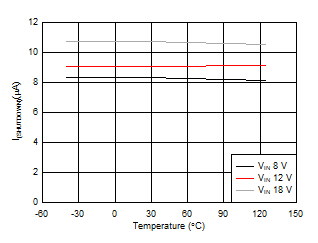
I(SHUTDOWN) | Shutdown mode current | VIN 8 V- 18 V, EN1 = 0 V, EN2 = 0 V, VCCX = 0 V | 9 | 12.5 | µA | |
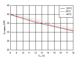
I(STANDBY) | Standby current | EN1 = 5 V, EN2 = 0 V, VOUT1, in regulation, no-load, not switching. VIN 8 V - 18 V. DEMB = GND |
35 | µA | ||
Or EN1 = 0 V, EN2 = 5 V, VOUT2 in regulation, no-load, not switching, VOUT2 connected to VCCX, DEMB = GND. |
42 | µA | ||||
VCC REGULATOR | ||||||
VCC(REG) | VCC regulation voltage | VIN = 6 V - 18 V, 0 - 150 mA, VCCX = 0 V |
4.75 | 5 | 5.25 | V |
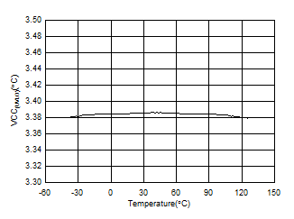
VCC(UVLO) | VCC under voltage threshold | VCC rising, VCCX = 0 V | 3.25 | 3.4 | 3.55 | V |
VCC(HYST) | VCC hysteresis voltage | VCCX = 0 V | 175 | mV | ||
ICC(LIM) | VCC sourcing current limit | VCCX = 0 V | 170 | 250 | mA | |
VDDA | ||||||
VDDA(REG) | Internal bias supply power | VCCX = 0 V | 4.75 | 5 | 5.25 | V |
VDDA(UVLO) | VDDA undervoltage lockout | VCC rising, VCCX = 0 V | 3.1 | 3.2 | 3.3 | V |
VDDA(HYST) | VDDA hysteresis voltage | VCCX = 0 V | 180 | mV | ||
R(VDDA) | VDDA resistance | VCCX = 0 V | 50 | Ω | ||
VCCX | ||||||
VCCX(ON) | VCC(ON) threshold | VCC rising | 4.1 | 4.3 | 4.4 | V |
R(VCCX) | VCCX resistance | VCCX = 5 V | 1 | Ω | ||
VCCX(HYST) | VCCX hysteresis voltage | 200 | mV | |||
OSCILLATOR SELECT THRESHOLDS | ||||||
2.2-MHz Oscillator select threshold | (OSC pin) | 2.4 | V | |||
440-kHz Oscillator select threshold | (OSC pin) | 0.4 | V | |||
CURRENT LIMIT | ||||||
V(CS1) | Current limit threshold1 | ILSET = VDDA, Measure from CS to VOUT |
66 | 73 | 80 | mV |
V(CS2) | Current limit threshold2 | ILSET = GND, Measure from CS to VOUT |
44 | 48 | 53 | mV |
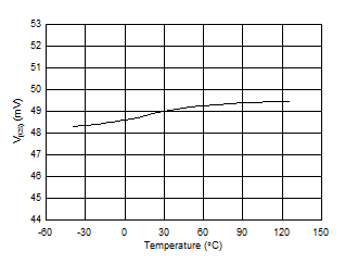
Current sense delay to output | 40 | ns | ||||
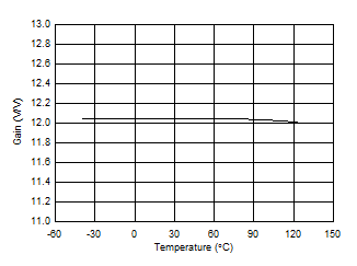
Current sense amplifier gain | 11.4 | 12 | 12.6 | V/V | ||
ICS(BIAS) | Amplifier input bias | 10 | nA | |||
75-mV current limit select threshold (ILSET) | 2.4 | V | ||||
75-mV current limit select threshold (ILSET) | 0.4 | V | ||||
RES | ||||||
I(RES) | RES current source | 20 | µA | |||
V(RES) | RES threshold | 1.2 | V | |||
Timer hIccup mode fault | 512 | cycles | ||||
RDS(ON) | RES pulldown | 5 | Ω | |||
OUTPUT VOLTAGE REGULATION | ||||||
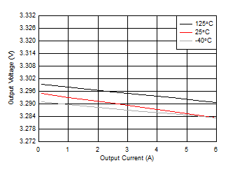
3.3 V | VIN = 3.8 V - 42 V | 3.273 | 3.3 | 3.327 | V | |
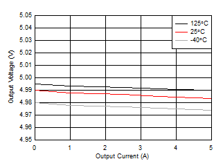
5 V | VIN = 5.5 V - 42 V | 4.95 | 5 | 5.05 | V | |
8 V | VIN = 8.5 V - 42 V | 7.92 | 8 | 8.08 | V | |
FEEDBACK | ||||||
VOUT1 select threshold 3.3-V Output | VDDA – 0.3 | V | ||||
VOUT2 select threshold 5 V | VDDA – 0.3 | V | ||||
Regulated Feedback Voltage | 1.19 | 1.2 | 1.21 | V | ||
FB(LOWRES) | Resistance to ground on FB for FB=0 detection | 500 | Ω | |||
FB(EXTRES) | Thevenin equivalent resistance at FB for external regulation detection | FB < 2 V | 5 | kΩ | ||
TRANSCONDUCTANCE AMPLIFIER | ||||||
Gm | Gain | Feedback to COMP | 1010 | 1200 | µS | |
FB | Input Bias Current | 15 | nA | |||
Transconductance Amplifier source current | COMP = 1 V, FB = 1.0 V | 100 | µA | |||
Transconductance Amplifier sink current | COMP = 1 V, FB = 1.4 V | 100 | µA | |||
POWER GOOD | ||||||
PG(UV) | PG1 and PG2 Under Voltage trip levels | Falling with respect to the regulation voltage | 90% | 92% | 94% | |
PG(OVP) | PG1 and PG2 Over Voltage trip levels | Rising with respect to the regulation voltage | 108% | 110% | 112% | |
PG(HYST) | Power Good hysteresis voltage | 3.4% | ||||
PG(VOL) | PG1 and PG2 | Open Collector, Isink = 2 mA | 0.4 | V | ||
PG(rdly) | OV Filter Time | VOUT rising | 25 | µs | ||
PG(fdly) | UV Filter Time | VOUT falling | 30 | µs | ||
HO GATE DRIVER | ||||||
VOLH | HO Low-state output voltage | IHO = 100 mA | 0.05 | V | ||
VOHH | HO High-state output voltage | IHO = -100 mA, VOHH = VHB - VHO | 0.07 | V | ||
trHO | HO rise time (10% to 90%) | CLOAD = 2700 pf | 4 | ns | ||
tfHO | HO fall time (90% to 10%) | CLOAD = 2700 pf | 3 | ns | ||
IOHH | HO peak source current | VHO = 0 V, SW = 0 V, HB = 5 V, VCCX = 5 V | 3.25 | Apk | ||
IOLH | HO peak sink current | VCCX = 5 V | 4.25 | Apk | ||
V(BOOT) | UVLO | HO falling | 2.5 | V | ||
Hysteresis | 110 | mV | ||||
I(BOOT) | Quiescent current | 3 | µA | |||
LO GATE DRIVER | ||||||
VOLL | LO Low-state Output Voltage | ILO = 100 mA | 0.05 | V | ||
VOHL | LO High-state Output voltage | ILO = -100 mA, VOHL = VCC - VLO | 0.07 | V | ||
trLO | LO rise time (10% to 90%) | CLOAD = 2700 pf | 4 | ns | ||
tfLO | LO fall time (90% to 10%) | CLOAD = 2700 pf | 3 | ns | ||
IOHL | LO peak source current | VCCX = 5 V | 3.25 | Apk | ||
IOLL | LO peak sink current | VCCX = 5 V | 4.25 | Apk | ||
ADAPTIVE DEAD TIME CONTROL | ||||||
V(GS-DET) | VGS detection threshold | VGS falling, no-load | 2.5 | V | ||
tdly1 | HO off to LO on dead time | 20 | ns | |||
tdly2 | LO off to HO on dead time | 15 | ns | |||
DIODE EMULATION | ||||||
VIL | DEM input low threshold | 0.4 | V | |||
VIH | FPWM input high threshold | 2.4 | V | |||
SW | zero cross threshold | –5 | mV | |||
ENABLE INPUTS EN1 AND EN2 | ||||||
VIL | Enable input low threshold | VCCX = 0 V | 0.4 | V | ||
VIH | Enable input high threshold | VCCX = 0 V | 2.4 | V | ||
Ilkg | Leakage | EN1, EN2 logic inputs only | 1 | µA | ||
SYN INPUT | ||||||
VIL | SYNIN input low threshold | 0.4 | V | |||
VIH | SYNIN input high threshold | 2.4 | V | |||
SYNIN input low frequency range 440 kHz | 350 | 550 | kHz | |||
SYNIN input low frequency range 2.2 MHz | 1800 | 2600 | kHz | |||
SYN OUTPUT | ||||||
VOH | SYN output high output voltage | Source -16 mA, VDDA = 5 V | 2.4 | V | ||
VOL | SYN Output low level output voltage | Sink 16 mA | 0.4 | V | ||
Phase between HO1 and HO2 | 180 | degrees | ||||
Duty Cycle | 50% | |||||
SOFT-START | ||||||
ISS | Soft-start current | 16 | 22 | 28 | µA | |
RDS(ON) | Soft-start pulldown resistance | 3 | Ω | |||
THERMAL | ||||||
TSD thermal shutdown | 175 | ºC | ||||
Thermal shutdown hysteresis | 15 | ºC |
PARAMETER | TEST CONDITIONS | MIN | TYP | MAX | UNIT | |
---|---|---|---|---|---|---|
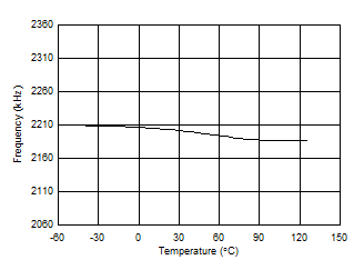
Oscillator frequency, 2.2 MHz | OSC = VDDA, VIN = 8 V – 18 V | 2060 | 2200 | 2340 | kHz | |
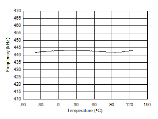
Oscillator frequency, 440 kHz | OSC = GND, VIN = 8 V – 18 V | 410 | 440 | 470 | kHz | |
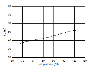
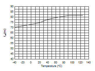
ton | Minimum on-time | 45 | ns | |||
toff | Minimum off-time | 100 | ns |
VIN 8-18 V | EN1 = EN2 = 12 V | 2.2 MHz |
VIN 8-18 V | EN1 = EN2 = 12 V |
VIN 6-18V | EN1 = EN2 = 12 V |
VCC Rising | EN1 = EN2 = 12 V |
VIN = 12 V | VCC Rising |
VIN = 12 V | ILSET = GND |
VIN 12 V | EN1 = 12 V | EN2 = GND |
VIN 12 V | OSC = VCC |
VIN 18 V |
VIN 8-18 V | EN1 = EN2 = 12 V | 2.2 MHz |
VIN 8-18 V | EN1 = 12 V, EN2 = 0 V | 2.2 MHz |
VCC Rising | EN1 = EN2 = 12 V |
VCC Rising |
VIN = 12 V | ILSET = VCC |
VCC Rising |
VIN 5.5 V - 42 V | EN1 = GND | EN2 = 12 V |
VIN 12 V | OSC = GND |
VIN 3.8 V |
The LM5140-Q1 is a dual-channel switching controller which features all of the functions necessary to implement a high efficiency buck power supply that can operate over a wide input voltage range. The LM5140-Q1 is configured to provide two independent outputs. VOUT1 can be a fixed 3.3 V, 5 V, or adjustable between 1.5 V to 15 V. VOUT2 can be a fixed 5 V, 8 V, or adjustable between 1.5 V to 15 V. This easy to use controller integrates high-side and low-side MOSFET drivers capable of sourcing 3.25 A and sinking 4.25-A peak . The control method is current mode control which provides inherent line feedforward, cycle-by-cycle current limiting, and ease-of-loop compensation. With the OSC pin connected to VDD the default oscillator frequency is 2.2 MHz. With the OSC pin grounded the oscillator frequency is 440 kHz. A synchronization pin allows the LM5140-Q1 to be synchronized to an external clock. Fault protection features include current limiting, thermal shutdown, and remote shutdown capability. The LM5140-Q1 incorporates features that simplify compliance with the CISPR and Automotive EMI requirements. The LM5140-Q1 gate drivers provide adaptive slew rate control and interleaved operation (180 degree output of phase) of the two controller channels. The 4-pin VQFN package with Wettable Flanks features an exposed pad to aid in thermal dissipation.
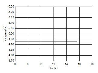
The LM5140-Q1 contains an internal high voltage VCC bias regulator that provides the bias supply for the PWM controller and the gate drivers for the external MOSFETs. The input pin (VIN) can be connected directly to an input voltage source up to 65 V. The output of the VCC regulator is set to 5 V. When the input voltage is below the VCC set-point level, the VCC output tracks VIN with a small voltage drop.
In high voltage applications, take extra care to ensure the VIN pin does not exceed the absolute maximum voltage rating of 70-V curing line or load transients. Voltage ringing on the VIN pin that exceeds the Absolute Maximum Ratings can damage the IC. Use care during PCB board layout and high quality bypass capacitors to minimize ringing.
The VCC regulator output current limit is 150 mA (minimum). At power up, the regulator sources current into the capacitors connected to the VCC pin. When the voltage on the VCC pin exceeds 3.4 V both output channels are enabled (if EN1 and EN2 are connected to a voltage source > 2.4 V) and the soft-start sequence begins. Both channels remain active unless the voltage on the VCC pin falls below the VCCUVLO threshold, of 3.2 V (typical) or the enable pins are switched to a low state. The LM5140-Q1 has two VCC pins; these pin must be connected together on the PCB. TI recommends that the VCC capacitor be split between the two VCC pins and connected to the respective PGND pins. The recommended range for the VCC capacitor is from 2.2 µF to 5 µF total.
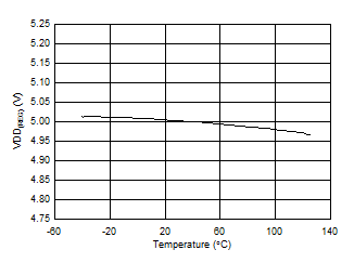
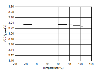
An internal 5-V linear regulator generates the VDDA bias supply. Bypass VDDA with a 100-nF or greater ceramic capacitor to ensure a low noise internal bias rail. Normally VDDA is 5 V, but there are two operating conditions where it regulates at 3.3 V. The first is in skip cycle mode with VOUT1 set to 3.3 V, and VOUT2 is disabled. The second is in a cold crank start-up where VIN is 3.8 V and VOUT1 is 3.3 V.
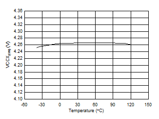
Internal power dissipation in the VCC Regulator can be minimized by connecting the VCCX pin to a 5-V output at VOUT1 or VOUT2 or to an external 5-V supply. If VCCX > 4.5 V, VCCX is internally connected to VCC and the internal VCC regulator is disabled. If VCCX is unused, it must be grounded. Never connect the VCCX pin to a voltage greater than 6.5 V.
The LM5140-Q1 has independent oscillators that generate the clock for each channel and can be programmed to 2.2 MHz or 440 kHz with the OSC pin. With the OSC pin connected to VDDA, both oscillators will be set to 2.2 MHz. With OSC grounded, they will both be set to 440 kHz. The state of the OSC pin is read and latched during VCC power up and thus cannot be changed until VCC drops below the VCCUVLO threshold. CLK1 is the clock for channel 1; CLK2 is for channel 2. CLK1 and CLK2 are 180º out of phase. The rising edge of SYNOUT always corresponds to the rising edge of CLK2 which is 180º out of phase with CLK1.
Under low VIN conditions when either of the high-side buck switch on time exceeds the programmed oscillator period, the LM5140-Q1 will extend the oscillator period of that channel until the PWM latch is reset by the current sense ramp exceeding the controller compensation voltage. In such an event, the oscillators (CLK1 and CLK2) operate independently and asynchronously until both channels can maintain output regulation at the programmed frequency.
The approximate input voltage level where this occurs is in Equation 1:
where
For example, if VOUT1 = 3.3 V and VOUT2 = 5 V and VIN drops to 6.41 V (see Equation 2).
In the above example, CLK2 frequency is required to drop to maintain regulation of VOUT2 while CLK1 can remain at the programmed frequency (refer to Figure 19). If VIN continues to drop, both CLK1 and CLK2 frequencies are reduced Figure 20.
Under high input voltage conditions (VIN > 20 V) when the buck switch on-time of either controller reaches the minimum on-time of 45 ns typical, the LM5140-Q1 reduces the oscillator frequency by skipping clock cycles for the appropriate channel.
Using the same output voltages as in the example above with VIN = 36 V, CLK1 drops to 1.1 MHz and CLK2 is 2.2 MHz, (refer to Figure 21), and SYNOUT is 2.2 MHz.
The SYNIN pin can be used to synchronize the LM5140-Q1 to an external clock. The synchronization range when the internal oscillator is set to 440 kHz is 374 kHz minimum to 506 kHz maximum. When the internal oscillator is set to 2.2 MHz, the synchronization range is 1.87 MHz to 2.53 MHz. If the synchronization feature is not being used, the SYNIN pin must be grounded.
CLK1 starts on the rising edge of the external synchronization clock (SYNIN). The HO1 pulse will follow approximately 110 ns after CLK1 due to internal delays (refer to Figure 22). Similarly, CLK2 generates the HO2 pulse after a short delay, and CLK2 is 180º out of phase with CLK1. SYNOUT always corresponds to the rising edge of CLK2.
Under low VIN conditions when the frequency must be reduced to maintain output voltage regulation, the SYNIN input function adapts as necessary. If VOUT1 can maintain regulation at the SYNIN frequency and VOUT2 cannot, then CLK1 remains synchronized to SYNIN and the CLK2 frequency is reduced (refer to Figure 23). If VOUT1 cannot maintain regulation at the SYNIN frequency, then the SYNIN signal is ignored and channel 1 frequency is reduced to maintain regulation. Channel 2 runs at the frequency determined by OSC pin or lower if required to maintain regulation on VOUT2 (refer to Figure 24).
At high VIN when pulse skipping is necessary, HO1 drops to 1.1 MHz and HO2 remains at 2.2 MHz (refer to Figure 25), and SYNOUT is 2.2 MHz.
The LM5140-Q1 contains two enable inputs, EN1 and EN2. The enable pins allow independent start-up and shutdown control of VOUT1 (EN1) and VOUT2 (EN2). The enable pins can be connected to a voltage as high as 70 V. If the enable input is greater than 2.4 V, the respective controller output is enabled. If the enable pins is pulled below 0.4 V, the respective output will be in shutdown. If both outputs are disabled the LM5140-Q1 is in a low IQ shutdown mode, with 9-µA typical current drawn from the VIN pin. TI does not recommend leaving either of the EN pins floating.
The LM5140-Q1 includes output voltage monitoring signals for VOUT1 and VOUT2 to simplify sequencing and supervision. The power good function can be used to enable circuits that are supplied by the corresponding voltage rail or to turn-on sequenced supplies. Each power good output (PG1 and PG2) switches to a high impedance open-drain state when the corresponding output voltage is in regulation. Each output switches low when the corresponding output voltage drops below the lower power good threshold (92% typical) or rises above the upper power good threshold (110% typical). A 25-µs deglitch filter prevents any false tripping of the power good signals due to transients. TI recommends pullup resistors of 10 kΩ (typical) from PG1 and PG2 to the relevant logic rail. PG1 and PG2 are asserted low during soft-start and when the corresponding buck converter is disabled by EN1 or EN2.
The LM5140-Q1 outputs can be independently configured for one of two fixed output voltages with no external feedback resistors or adjusted to the desired voltage using external resistor dividers. VOUT1 can be configured as a 3.3-V output by connecting the FB1 pin to VDDA, or a 5-V output by connecting the FB1 pin to ground with a maximum resistance of 500 Ω. VOUT2 can be configured as either a 5-V output or 8-V output. For a 5-V output at VOUT2, connect the FB2 pin to VDDA. For a fixed 8-V output at VOUT2 connect FB2 to ground with a maximum resistance of 500 Ω. The FB1 and FB2 connections (either VDDA or GND) are detected during power up. The configuration setting is latched and can not be changed until the LM5140-Q1 is powered down with VCC falling below VCC(UVLO) (3.4 V typical) and then powered up again.
Alternative output voltages can be set external resistive dividers from output to the FB pins. The output voltage adjustment range is between 1.5 V and 15 V. The regulation threshold at the FB pin is 1.2 V (VREF). To calculate RFB1 and RFB2 use Equation 3, refer to Figure 26:
The recommend value for R(FB1) is between 10 kΩ to 20 kΩ.
The Thevenin equivalent impedance of the resistive divider connected to the FB pins must be greater than 5 kΩ for the LM5140-Q1 to detect the divider and set the channel to the adjustable output mode.
If a low IQ mode is required, take care when selecting the external resistors. The extra current drawn from the external divider is added to the LM5140-Q1 I(STANDBY) current (35 µA typical). The divider current reflected to VIN is divided down by the ratio of VOUT/VIN. For example, if VOUT is set to 5.5 V with RFB1 10 kΩ, and RFB2 = 35.8 kΩ (use 35.7 kΩ), the input current at VIN required to supply the current in the feedback resistors is:
VIN = 12 V
If one output is enabled and the other disabled, VCC output will be in regulation. The HB pin voltage of the disabled channel will charge to VCC through the boot strap diode. As a result, the HO driver bias current (approximately 3 µA) can charge the disabled channel VOUT to approximately 2.2 V. If this is not desired, a load resistor (100 kΩ) can be added to the output that is disabled to maintain a low voltage OFF-state.
There are two limitations to the minimum output voltage adjustment range: the LM5140-Q1 voltage reference 1.2 V and the minimum switch node pulse width, tSW.
The minimum controllable voltage at the switch node (tSW) limits the voltage conversion ratio (VOUT/VIN). For fixed-frequency PWM operation, the voltage conversion ratio must meet Equation 7:
where
If the desired voltage conversion ratio does not meet the above condition, the controller transitions from fixed frequency operation into a pulse skipping mode to maintain regulation of the output voltage.
For example if the desired output voltage is 3.3 V with a VIN of 20 V and operating at 2.2 MHz, the voltage conversion ratio test is in Equation 8:
For Wide VIN applications and lower output voltages, an alternative is to use the LM5140-Q1 with 440-kHz oscillator frequency. Operating at 440 kHz, the limitation with the minimum ton time is less significant. For example, if a 1.8-V output is required with a VIN of 50 V (see Equation 9):
There are two methods to sense the inductor current of the buck converters. The first is using current sense resistor in series with the inductor and the second is to use the DC resistance of the inductor (DCR sensing). Figure 27 illustrates inductor current sensing using a current sense resistor. This configuration continuously monitors the inductor current providing accurate current-limit protection. For the best current-sense accuracy and overcurrent protection, use a low inductance ±1% tolerance current-sense resistor between the inductor and output, with a Kelvin connection to the LM5140-Q1 sense amplifier.
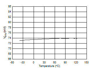
The LM5140-Q1 provides two user selectable current limit levels of 48 mV and 73 mV. If the ILSET pin is connected to VDDA, the current limit threshold is 73 mV. When the ILSET pin is connected to ground, the current limit set point is 48 mV. The ILSET pin is monitored during power up and the setting is latched. To change the setting, VIN power must be removed from the controller allowing the VCC voltage to drop below VCC(UVLO).
If the peak differential current signal sensed from CS to VOUT exceeds the user selectable current limit level of 48 mV or 73 mV, the current limit comparator immediately terminates the HO output for cycle-by-cycle current limiting.
where
For high-power applications which do not require high accuracy current-limit protection, DCR sensing may be preferable. This technique provides lossless and continuous monitoring of the output current using an RC sense network in parallel with the inductor. Using an inductor with a low DCR tolerance, the user can achieve a typical current limit accuracy within the range of 10% to 15% at room temperature.
Components RSC and CCS in Figure 28 create a low-pass filter across the inductor to enable differential sensing of the voltage drop across inductor DCR. When RCS × CCS is equal to LOUT/LDCR, the voltage developed across the sense capacitor, CS, is a replica of the inductor DCR voltage waveform. Choose the capacitance of CCS to be greater than 0.1 μF to maintain a low impedance sensing network, thus reducing the susceptibility of noise pickup from the switch node. Carefully observe the PCB layout guidelines to ensure the noise and DC errors do not corrupt the differential current-sense signals applied across the CS and VOUT pins.
The voltage drop across CCS in Equation 11:
RCSCCS = LOUT/LDCR → accurate DC and AC current sensing.
If the RC time constant is not equal to the LOUT/LDCR time constant, there is an error.
RCSCCS > LOUT/LDCR → DC level still correct, the AC amplitude is attenuated.
RCSCCS < LOUT/LDCR → DC level still correct, the AC amplitude is amplified.
Each channel of the LM5140-Q1 has an independent high-gain transconductance amplifier which generates an error current proportional to the difference between the feedback voltage and an internal precision reference (1.2 V). The output of each transconductance amplifier is connected to the COMP pin allowing the user to provide external control loop compensation. Generally for current mode control a type II network is recommended.
The LM5140-Q1 provides internal slope compensation to ensure stable operation with duty cycle greater than 50%. To correctly use the internal slope compensation, the inductor value must be calculated based on the following guidelines (Equation 12 assumes an inductor ripple current of 30%):
The LM5140-Q1 includes an optional hiccup mode protection function that is enabled when a capacitor is connected to the RES pin. In normal operation the RES capacitor is discharged to ground. If 512 cycles of cycle-by-cycle current limiting occur on a either channel, the SS pin capacitor of that channel is pulled low and the HO and LO outputs are disabled (refer to Figure 29). A 20-μA current source begins to charge the RES capacitor. When the RES pin charges to 1.2 V, the RES pin is pulled low and the SS capacitor begins to charge. The 512 cycle hiccup counter is reset if 4 consecutive switching cycles occur without exceeding the current limit threshold. Separate hiccup counters are provided for each channel, but the RES pin is shared by both channels. One channel can be in the hiccup protection mode while the other operates normally. In the event that both channels are in an overcurrent condition triggering hiccup protection, the last hiccup counter to expire pulls RES low and starts the RES capacitor charging cycle. Both channels then restart together when RES=1.2 V. If RES is connected to VDDA at power up, the hiccup function is disabled for both channels.
The controller is in forced PWM (FPWM) continuous conduciton mode when the DEMB pin is connected to VDDA. In this mode the SS pin is clamped to a level 200 mV above the feedback voltage to the internal error amplifier. This ensures that SS can be pulled low quickly during a brief overcurrent event and prevent overshoot of VOUT when the overcurrent condition is removed.
If DEMB=0 V, the controller operates in diode emulation with light loads (discontinous conduction mode) and the SS pin is allowed to charge to VDDA. This reduces the quiescent current of the LM5140-Q1. If 32 or more cycle-by-cycle current limit events occur, the SS pin is clamped to 200 mV above the feedback voltage to the internal error amplifier until the hiccup counter is reset. Thus, if a momentary overload occurs that causes at least 32 cycles of current limiting, the SS capacitor voltage is slightly higher than the FB voltage and controls VOUT during recovery.
The LM5140-Q1 operates with peak current mode control such that the feedback compensation voltage is proportional to the peak inductor current. During no-load or light load conditions, the output capacitor discharges very slowly. As a result the compensation voltage does not demand a driver output pulses on a cycle-by-cycle basis. When the LM5140-Q1 controller detects that there have been 16 missing switching cycles, it enters Standby Mode and switches to a low IQ state to reduce the current drawn from VIN. For the LM5140-Q1 to go into a Standby Mode, the controller must be programmed for diode emulation (DEMB pin < 0.4 V). The typical IQ in Standby Mode is 35 µA with VOUT1 regulating at 3.3 V and VOUT2 disabled. With VOUT1 disabled and VOUT2 regulating to 5 V, the Standby Mode current is 42 μA. With both channels in standby mode (VOUT1 = 3.3 V and VOUT2 = 5 V) the VIN current is 75 μA. Using external feedback resistors add additional load to VOUT and significantly increase the Standby Mode VIN current.
The soft-start feature allows the regulator to gradually reach the steady-state operating point, thus reducing start-up stresses and surges. The LM5140-Q1 regulates the FB pin to the SS pin voltage or the internal 1.2-V reference, whichever is lower. At the beginning of the soft-start sequence when SS = 0 V, the internal 20-μA soft-start current source gradually increases the voltage on an external soft-start capacitor connected to the SS pin, resulting in a gradual rise of the FB and output voltages.
The controller is in the forced PWM (FPWM) mode when the DEMB pin is connected to VDDA. In this mode, the SS pin is clamped at 200 mV above the feedback voltage to the internal error amplifier. This ensures that SS can be pulled low quickly during brief overcurrent events and prevent overshoot of VOUT during recovery. SS can be pulled low with an external circuit to stop switching, but this is not recommended. Pulling SS low results in COMP being pulled down internally as well. If the controller is operating in FPWM mode (DEMB = VDDA), LO remains on and the low-side MOSFET discharges the VOUT capacitor resulting in large negative inductor current. When the LM5140-Q1 pulls SS low internally due to a fault condition, the LO gate driver is disabled.
A fully synchronous buck regulator implemented with a free-wheel MOSFET rather than a diode has the capability to sink current from the output in certain conditions such as light load, overvoltage, and prebias start-up. The LM5140-Q1 provides a diode emulation feature that can be enabled to prevent reverse (drain to source) current flow in the low-side free-wheel MOSFET. When configured for diode emulation, the low-side MOSFET is disabled when reverse current flow is detected. The benefit of this configuration is lower power loss at no load or light load conditions and the ability to turn on into a prebiased output without discharging the output. The negative effect of diode emulation is degraded light load transient response times. Enabling the diode emulation feature is recommended to allow discontinuous conduction operation. The diode emulation feature is configured with the DEMB pin. To enable diode emulation, connect the DEMB pin to ground or leave the pin floating. If continuous conduction operation is desired, the DEMB pin must be tied to VDDA.
The LM5140-Q1 contains a N-channel MOSFET gate drivers and an associated high-side level shifter to drive the external N-channel MOSFET. The high-side gate driver works in conjunction with an external bootstrap diode DBST, and bootstrap capacitor CBST, refer to Figure 30. During the on-time of the low-side MOSFET, the SW pin voltage is approximately 0 V and CBST is charged from VCC through the DBST. A 0.1-μF or larger ceramic capacitor, connected with short traces between the BST and SW pin, is recommended.
The LO and HO outputs are controlled with an adaptive dead-time methodology which ensures that both outputs (HO and LO) are never enabled at the same time, preventing cross conduction. When the controller commands LO to be enabled, the adaptive dead-time logic first disables HO and waits for the HO-SW voltage to drop below 2.5 V typical. LO is then enabled after a small delay (HO fall to LO rise delay). Similarly, the HO turn-on is delayed until the LO voltage has dropped below 2.5 V. HO is then enabled after a small delay (LO fall to HO rise delay). This technique ensures adequate dead-time for any size N-channel MOSFET device or parallel MOSFET configurations. Caution is advised when adding series gate resistors, as this may decrease the effective dead-time. Eachof the high and low-side drivers have an independent driver source and sink output pins. This allows the user to adjust drive strength to optimize the switching losses for maximum efficiency and control the slew rate for reduced EMI. The selected N-channel high-side MOSFET determines the appropriate boost capacitance values CBST in the Figure 30 according to Equation 13.
where
Choose ΔVBST such that the available gate-drive voltage is not significantly degraded when determining CBST. A typical range of ΔVBST is 100 mV to 300 mV. The bootstrap capacitor must be a low-ESR ceramic capacitor. A minimum value of 0.1 µF to 0.47 µF is best in most cases. Take care when choosing the high-side and low-side MOSFET devices with logic level gate thresholds.
NOTE
Information in the following applications sections is not part of the TI component specification, and TI does not warrant its accuracy or completeness. TI’s customers are responsible for determining suitability of components for their purposes. Customers should validate and test their design implementation to confirm system functionality.
The LM5140-Q1 is a synchronous buck controller used to convert a higher input voltage to two lower output voltages. The following design procedure can be used to select external component values. Alternately, the WEBENCH® software may be used to generate a complete design. The WEBENCH software uses an iterative design procedure and accesses a comprehensive database of components when generating a design. This section presents a simplified discussion of the design process. In addition to the WEBENCH software the LM5140ADESIGN-CALC.XIXS quick start Excel calculator is available at www.ti.com.
For this design example, the intended input, output and performance parameters are shown in Table 1.
DESIGN PARAMETER | EXAMPLE VALUE |
---|---|
Input voltage range (steady-state) | 8 V to 18 V |
Transient | 42 V |
Cold crank | 3.8 V |
Output voltage | 3.3 V |
Output current | 6 A |
Operating frequency | 2.2 MHz |
Output voltage regulation | ± 1% |
Standby current, one output enabled, no-load | < 35 µA |
Shutdown current | 9 µA |
For peak current mode control, sub-harmonic oscillation occurs with a duty cycle greater than 50% and is characterized by alternating wide and narrow pulses at the SW pin. By adding a slope compensating ramp equal to at least one-half the inductor current down-slope, any tendency toward sub-harmonic oscillation is damped within one switching cycle. For design simplification, the LM5140-Q1 has an internal slope compensation ramp added to the current sense signal.
For the slope compensation ramp to dampen sub-harmonic oscillation, the inductor value should be calculated based on the following guidelines (Equation 14 assumes an inductor ripple current 30%):
A standard inductor value of 1.5 µH is selected.
The maximum peak-to-peak inductor current is calculated in Equation 18 through Equation 21:
When calculating the current sense resistor, the maximum output current capability (IOUTMAX) must be at least 20% higher than the required full load current to account for tolerances, ripple current, and load transients. For this example, 120% of the 6.41-A peak inductor current calculated in the previous section (Ipk) is 7.69 A. The current sense resistor value can be calculated using Equation 22 and Equation 23:
where
The Rsense value selected is 9 mΩ
Carefully observe the PCB layout guidelines to ensure that noise and DC errors do not corrupt the differential current sense signals between the CS and VOUT pins. Place the sense resistor close to the devices with short, direct traces, creating Kelvin-sense connections between the current-sense resistor and the LM5140-Q1.
The propagation delays through the current limit comparator, logic, and external MOSFET gate drivers allow the peak current to increase above the calculated current limit threshold. For a total propogation delay of tdlyTOTAL, the worst case peak current through the inductor with the output is shorted can be calculated from Equation 24:
From the Electrical Characteristics, tdlyTOTAL 40 ns (see Equation 25)
Once the peak current and the inductance parameters are known, the inductor can be chosen. An inductor with a saturation current greater than Ipkshortckt (8.59 Apk) should be selected.
In a switch mode power supply, the minimum output capacitance is typically selected based on the capacitor ripple current rating and the load transient requirements. The output capacitor must be large enough to absorb the inductor energy and limit over voltage when transitioning from full-load to no-load, and to limit the output voltage undershoot during no-load to full load transients. The worst-case load transient from zero to full load occurs when the input voltage is at the maximum value and a current switching cycle has just finished. The total output voltage drop VOUTUV is the sum of the voltage drop while the inductor is ramping up to support the full load and the voltage drop before the next pulse can occur.
The output capacitance required to maintain the minimum output voltage drop VOUTUV can be calculated in Equation 26 and Equation 27:
where
For this example a total of 293 µF of capacitance is used, three 82-µF aluminum capacitors for energy storage and one 47-µF low ESR ceramic capacitor to reduce high frequency noise.
Generally, when sufficient capacitance is used to satisfy the undershoot requirement, the overshoot during a full-load to no-load transient will also be satisfactory. After the output capacitance has been selected, calculate the output ripple current and verify that the ripple current is within the capacitor ripple current ratings.
For this design, the output ripple current is calculated in Equation 28 and Equation 29:
A power supply input typically has a relatively high source impedance at the switching frequency. Good-quality input capacitors are necessary to limit the ripple voltage at the VIN pin while supplying most of the switch current during the buck switch on-time. When the buck switch turns on, the current drawn from the input capacitor steps from zero to the valley of the inductor current waveform, then ramps up to the peak value, and then drops to the zero at turnoff.
Average input current can be calculated from the total input power required to support the loads at VOUT1 and VOUT2 in Equation 30:
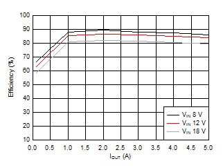
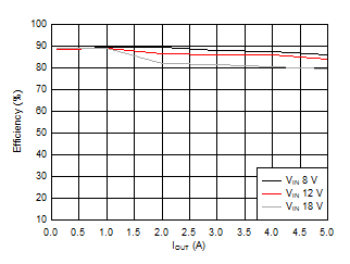
The efficiency η is assumed to be 83% for this design example, yielding total input power:
The ripple voltage on the input capacitors is reduced significantly with a dual-channel operation because each channel operates 180º out of phase from the other. Capacitors connected in parallel should be evaluated for their RMS current rating. The ripple current splits between the input capacitors based on the relative impedance of the capacitors at the switching frequency.
The input capacitors must be selected with sufficient RMS current rating and the maximum voltage rating. The input ripple current with one channel operating is calculated in Equation 34 and Equation 35:
Switching regulators exhibit negative input impedance, which is lowest at the minimum input voltage. An under-damped LC filter exhibits a high output impedance at the resonant frequency of the filter. For stability, the filter output impedance must be less than the absolute value of the converter input impedance.
EMI Filter Design Steps:
By calculating the first harmonic current from the Fourier series of the input current waveform and multiplying it by the input impedance (the impedance is defined by the existing input capacitor CIN), a formula can be derived to obtain the required attenuation (see Equation 38 and Equation 39):
Vmax is the allowed dBμV noise level for the particular EMI standard, CIN is the existing input capacitors of the buck converter. For this application 10 µF was selected. Dmax is the maximum duty cycle. Ipk is the peak inductor current and for filter design purposes, the current at the input can be modeled as a squarewave. The EMI filter capacitor Cf is determined from:
For this application, Cf was chosen to be 1 µF. Adding an input filter to a switching regulator modifies the control-to-output transfer function. The output impedance of the filter must be sufficiently small such that the input filter does not significantly affect the loop gain of the buck converter. The impedance peaks at the filter resonant frequency. The resonant frequency of the filter is given by Equation 42 and Equation 43:
The purpose of Rd is to reduce the peak output impedance of the filter at the resonant frequency. The capacitor Cd blocks the DC component of the input voltage to avoids excessive power dissipation in Rd. The capacitor Cd must have lower impedance than Rd at the resonant frequency with a capacitance value greater than the input capacitor CIN. This prevents the CIN from interfering with the cutoff frequency of the main filter. Added damping is needed when the output impedance is high at the resonant frequency ( Q of filter formed by CIN and Lf is too high): An electrolytic cap Cd can be used as damping device, with the value of Equation 44:
Cd = 4 × 10 µF, a 47-µF capacitor was selected and Rd is chosen using Equation 45 and Equation 46:
The LM5140-Q1 gate drivers are powered by the internal 5-V VCC bias regulator. To reduce power dissipation in the controller and improve efficiency, the VCCX pin which must be connected to 5-V output or an external 5-V bias supply. The MOSFETs used with the LM5140 require a logic-level gate threshold with on-resistance specified with VGS = 4.5 V or lower.
The four MOSFETs must be chosen with a VDS rating to withstand the maximum VIN voltage plus supply voltage transients and spikes (ringing). For automotive applications, the maximum VIN occurs during a load dump and the voltage can surge to 42 V under some conditions. A MOSFET with a VDS rating of 60 V would meet most application requirements. The N-channel MOSFETs must be capable of delivering the average load current plus peak ripple current during switching.
The high-side MOSFET losses are associated with the RDS(ON) of the MOSFET and the switching losses.
The losses in the low-side MOSFET include the RDS(ON) losses, the dead time losses, and losses in the MOSFETs internal body diode. The body diode conducts the inductor current during the dead time before the rising edge of the switch node. Minority carriers are injected into and stored in the body diode PN junction. As the high-side FET begins to turn on, a negative current must first flow through the diode to remove the stored charge before the diode can be reverse biased. During this time, the high-side MOSFET drain-source voltage remains at VIN until all the diode minority carriers are removed. Then the diode begins to block negative voltage and the reverse current continues to flow to charge the depletion capacitance of the body diode junction. The total charge required to reverse bias the diode is called reverse-recovery charge Qrr. The power loss in the low-side MOSFET can be calculated from Equation 49 and Equation 50:
where
Table 2 provides parameters for several MOSFETs that have tested in the LM5140-Q1 evaluation module.
MANUFACTURER | PART NUMBER | VDS (V) | ID (A) | QgMAX (nC) VGS = 4.5 V |
RDSON MAX (mΩ) VGS = 4.5 |
COSS /MAX | APPLICATION |
---|---|---|---|---|---|---|---|
VISHAY | SQJ850EP | 60 | 24 | 30 | 32 | 215 | Automotive High Power |
VISHAY | SQ7414EN | 60 | 5.6 | 25 | 36 | 175 | Automotive Low Power |
Texas Instruments | CSD18534Q5A | 60 | 13 | 11.1 | 12.4 | 217 | Industrial |
Figure 33 shows the high current driver outputs with independent source and current sink pins for slew rate control. Slew rate control enables the user to adjust the switch node rise and fall times which can reduce the conducted EMI in the FM radio band (30 MHz to 108 MHz). Using the LM5140-Q1 EVM, conducted emission were measured in accordance with CISPR 25. Figure 34 shows the measured results without slew rate control. The conducted EMI results with slew rate control are shown in Figure 35.
Referring to Figure 34 and Figure 35 a 10-dB reduction in conduction emissions in the FM band is attained by using slew rate control. This can reduce the size and cost of the EMI filters.
For peak current mode control, sub-harmonic oscillation occurs with a duty cycle greater than 50% and is characterized by alternating wide and narrow pulses at the SW pin. By adding a compensating ramp equal to the down-slope of the inductor current, any tendency toward sub-harmonic oscillation is damped within one switching cycle.
In time-domain analysis, the steady-state inductor current starts and ends at the same value during one clock cycle. If the magnitude of the end-of-cycle current error, dI1, caused by an initial perturbation, dI0, is less than the magnitude of dI0 or dI1/dI0 > –1, the perturbation naturally disappears after a few cycles, refer to Figure 36. When dI1/dI0 < –1, the initial perturbation does not disappear resulting in sub-harmonic oscillation in steady-state operation. By choosing K > 1 , sub-harmonic oscillation is avoided.
The relationship between Q and K factor is illustrated graphically in Figure 37.
The minimum value of K is 0.5. This is the same as time domain analysis result. When K < 0.5, the regulator is unstable. High gain peaking at 0.5 results in sub-harmonic oscillation at FSW//2. When K = 1, one-cycle damping is realized and Q is equal to 0.673 at this point. A higher K factor may introduce additional phase shift by moving the sampled gain inductor pole closer to the crossover frequency but helps reduce noise sensitivity in the current loop.
The open-loop gain is defined as the product of modulator and feedback transfer functions. When plotted on a dB scale, the open loop gain is shown as the sum of modulator gain and feedback gain.
DC modulator gain is calculated in Equation 52:
where
The modulator gain plus power stage transfer function with an embedded current loop is shown in Equation 53. The equation included the sample gain at FSW/2 (ωn), which is caused by sampling effect of current mode control.
Because the loop cross over frequency is well below sample gain effects, Equation 54 can be simplified as one pole and a one zero system as shown in Equation 55
A type ll compensator using an transconductance error amplifier (EA) Gm is shown in Figure 38. The dominant pole of the EA open-loop gain is set by the EA output resistance, RAMP, and effective bandwidth-limiting capacitance, CO as follows:
The EA high frequency pole is neglected in the above expression. The compensator transfer function from the output voltage to COMP, including the gain contribution from the feedback resistor divider network, is calculated in Equation 57:
where
Typically RCOMP <<RAMP and CCOMP>> (CO) so the approximations are valid.
The error amplifier compensation components create a pole at the origin, a zero, and a high frequency pole.
The procedure for choosing compensation components for a stable closed loop is:
The value selected for RCOMP is 22.6 kΩ
The value selected for CCOMP is 10 nF