-
Interfacing the C2000 With an AFE03x: B-FSK Example SPRAC94D September 2018 – March 2022 AFE030 , AFE031 , TMS320F28075 , TMS320F28075-Q1 , TMS320F28076 , TMS320F28374D , TMS320F28374S , TMS320F28375D , TMS320F28375S , TMS320F28375S-Q1 , TMS320F28376D , TMS320F28376S , TMS320F28377D , TMS320F28377D-EP , TMS320F28377D-Q1 , TMS320F28377S , TMS320F28377S-Q1 , TMS320F28379D , TMS320F28379D-Q1 , TMS320F28379S
-
Interfacing the C2000 With an AFE03x: B-FSK Example
- Trademarks
- 1 FSK Overview
- 2 Hardware Overview
- 3 Interfacing With the AFE03x
- 4 Transmit Path
- 5 Receive Path
- 6 Interfacing With a Power Line
- 7 Summary
- 8 References
- 9 Schematics
- 10Revision History
- IMPORTANT NOTICE
Interfacing the C2000 With an AFE03x: B-FSK Example
Trademarks
C2000 and Code Composer Studio are trademarks of Texas Instruments.
All trademarks are the property of their respective owners.
1 FSK Overview
Frequency Shift Keying (FSK) is a modulation scheme that utilizes discrete changes of frequency to transmit and receive digital data. One of the simplest subsections of this modulation scheme, and also the modulation used in this demo, is called Binary Frequency Shift Keying (BFSK).
In this scheme, the system is switching between two discrete frequencies: the Mark Frequency (“1”) and the Space Frequency (“0”). These frequencies correlate directly to the bit value of the transmitted data.
Figure 1-1 shows what this looks like in the time domain.
 Figure 1-1 Binary FSK in the Time
Domain
Figure 1-1 Binary FSK in the Time
DomainFigure 1-2 shows an example of a simplified FSK transmitter where the block consists of two oscillators with an internal clock as well as an input binary sequence to control the position of the switch.
 Figure 1-2 Transmitter Example
The two oscillators, producing a higher (space) and a lower (mark) frequency signals, are connected to a switch along with an internal clock. A clock is applied internally to both oscillators to avoid phase discontinuities of the output waveform during the transmission of the message. The binary input sequence is applied to choose the frequencies according to the binary input. In this case, binary "0" corresponds to the output of the space frequency and binary "1" corresponds to the output of the mark frequency.
Figure 1-3 shows an example of a simplified FSK receiver to convert a received signal back into the desired digital information.
 Figure 1-3 Receiver Example
A FSK waveform is initially filtered and then mixed with signals of the desired mark (fmark ) and space (fspace ) frequencies. The output is run through a detector algorithm and the results are compared to decipher if the signal being received pertains to a mark, binary "1", or space, binary"0". Additional functionality is included to decipher received bits, based on the duration of the received mark or space signal, and handle the boundaries between consecutive bits.
This is a simple overview on how FSK works. The following sections discuss how this is implemented on a C2000 device.
2.1 Block Diagram
Figure 2-3 shows a block diagram of the system. In this example, not all of the connections have been utilized, but all are present on the BoosterPack for future development.
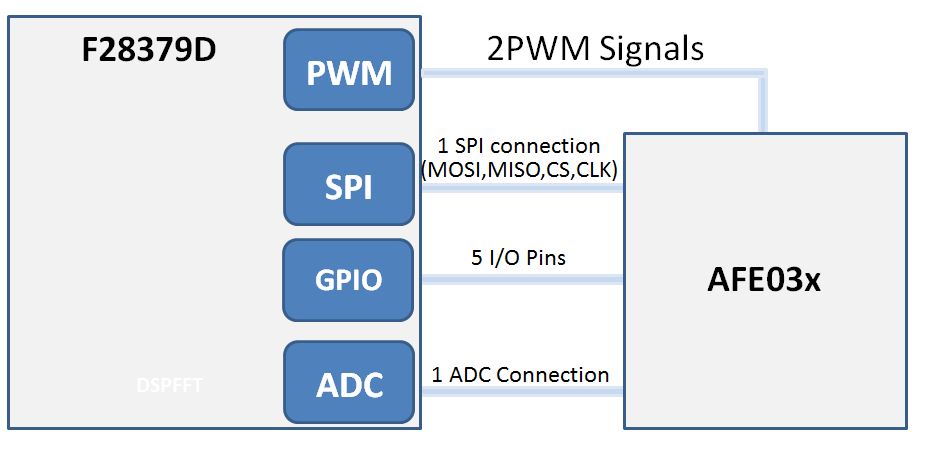 Figure 2-3 C2000 and AFE031 Block Diagram
The AFE has multiple internal registers that allow configuration of the internal components of the AFE chip, including filter selection, gain selection, and mode selections. These registers can be accessed using the SPI peripheral.
The AFE also has various GPIOs that allow the MCU to set the AFE into certain modes, as well as receive interrupts for critical events on the AFE. The ADC connection allows the MCU to receive or sample an input signal. The PWM signals provide a way to create an output for the AFE. Currently the AFE031 supports two modes of data transmission, PWM mode and DAC mode. An explanation and implementation of both of these modes can be found in Section 3.
2.2 Hardware Setup
There are a few things that need to be done so that the hardware can be debugged correctly. Power is supplied to the BOOSTXL-AFE031 test board via the 15 V jumper. The BoosterPack has a regulator that will supply power to the LaunchPad connected. Figure 2-4 shows a close up of the 15 V headers.
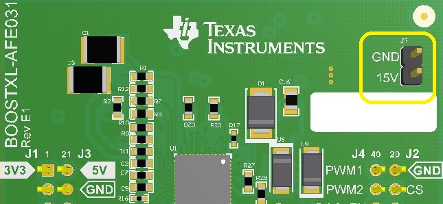 Figure 2-4 BOOSTXL-AFE031 Power Pins
The wire connected to the right input of the terminal block shown in Figure 2-5 will be the line that the transmitted output or received input FSK signal resides on, depending on whether the system is set up as a transmitter or receiver. The wire connected to the left input of the terminal block is the ground line. These lines can then be connected to some coupling circuitry or directly to another BOOSTXL-AFE031 terminal block for controlled testing, TX/RX to TX/RX and GND to GND.
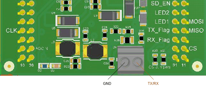 Figure 2-5 BOOSTXL-AFE031 Terminal Block Connections
Since the BoosterPack is supplying power to the launchPad, the PC USB interface needs to be isolated. Header jumpers JP1, JP2, and JP3 on the launchpad need to be removed to enable electrical isolation. Figure 2-6 is a close up of the location of the headers.
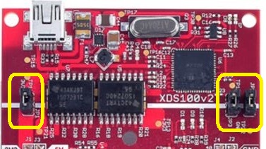 Figure 2-6 F28379D Jumper Configuration
When using the system as a FSK receiver, the LaunchPad needs 5 V to power the C2000 ADC. With the LaunchPad being isolated from the PC USB interface, the 5 V power rail needs to be generated by stepping up the supplied 3.3 V. Header JP6 on the LaunchPad needs to be added to enable the step-up regulator. Figure 2-7 is a close up of the location of the header.
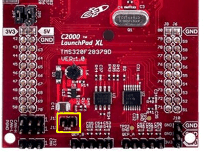 Figure 2-7 F28379D JP6 Location
When using the system as a receiver, make sure that the F28379D LaunchPad is version 2.0 or greater. Earlier versions (Ver 1.1 and 1.2) have an issue with the ADCIN pin that is connected to the BOOSTXL-AFE031. For more information, see the LAUNCHXL-F28379D Overview revisions section.
When using the transmitter solution in conjunction with the receiver solution, the complete system connection should look similar to what is shown in Figure 2-8.
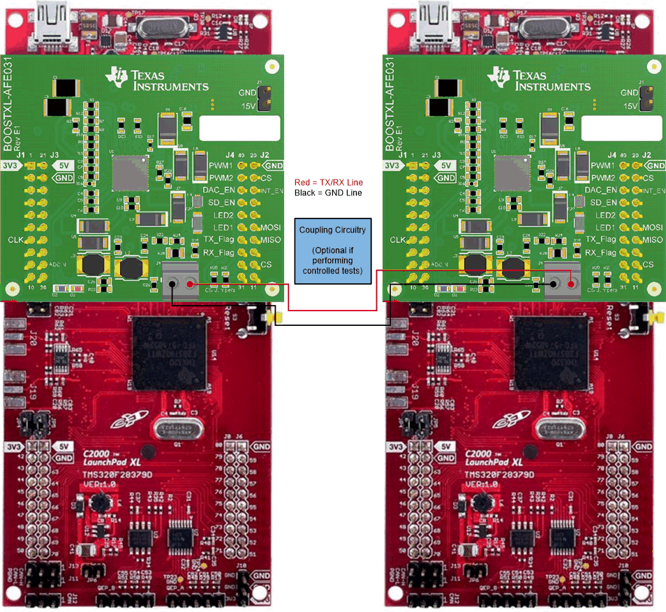 Figure 2-8 TX-RX Solution System
