-
How to Design One Battery Tester for a Wide Range of Sizes, Voltages and Form Factors
How to Design One Battery Tester for a Wide Range of Sizes, Voltages and Form Factors
Shaury Anand
With lithium-ion batteries found in both small electronic devices and much larger applications such as electric vehicles and electricity grids, they naturally span a wide range of sizes, voltages and form factors. But this breadth means that battery manufacturers have to buy and maintain testing solutions for each battery type, and the associated capital investment becomes significant, directly contributing as much as 20% to the final cost of the batteries.
There’s a clear need for a cost-effective, multirange test solution that can handle a broader range of battery voltages, capacities and physical sizes. This article describes the benefits of a digital control loop battery tester and includes an example of a flexible and cost-effective battery test design. For an overview on battery testing design challenges, read our white paper, "Designing an Accurate, Multifunction Lithium-Ion Battery-Testing Solution."
Benefits of a digital control loop
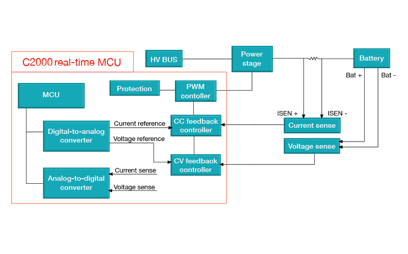
The main functions of a battery tester are to control and monitor the charging and discharging of a battery. Figure 1 shows a functional block diagram of a switching-type battery tester. It is possible to implement the control part in either analog or digital. In the analog implementation, a pulse-width modulation (PWM) controller regulates the output voltage or current flowing through the high- and low-voltage supplies. The protection circuit is integrated in the PWM controller. The constant-current and constant-voltage feedback loop drives the reference input of the PWM controller to precisely control the output current and voltage. A 16-bit digital-to-analog converter (DAC) connected to feedback controllers sets the output current and voltage. Finally, a precision 16-bit analog-to-digital converter (ADC) monitors the battery voltage and current.
 Figure 1 Battery tester block diagram
In the digital implementation, the microcontroller (MCU) performs all the functions inside the red box shown in Figure 1. With the C2000™ real-time control MCU, you can generate 16-bit PWM and use its comparators to implement protection algorithms. The MCU uses the ADC output data to implement current and voltage controllers. Because the controllers are in the digital domain, this architecture doesn’t require a precision 16-bit DAC. A 12-bit on-chip ADC can achieve a control accuracy less than ±0.05%, which is sufficient for cost-optimized battery test systems. However, the implementation requires an external 16-bit precision in the feedback to achieve a control accuracy better than ±0.01%. A digital solution easily achieves flexibility with accuracy; performance and cost differences will depend only on whether you choose to use an external 16-bit ADC or internal 12-bit ADC in the feedback. The efficient use of the MCU in this implementation results in more than 30% savings in the bill of materials.
| Multiple voltages, capacities and sizes. One reference design. | |

|
Use our single, flexible design to test a broad range of battery voltages, capacities and battery sizes. |
Today’s test equipment is designed for a specific battery type. Larger batteries require higher amounts of current and thus a battery tester with multiple channels connected in parallel. But if a battery manufacturer is producing smaller batteries with lower current requirements, they typically use the testers specifically optimized for lower current levels, while the high-current battery testers remain idle. Having a tester capable of testing both smaller and larger batteries reduces this redundancy and helps bring down the overall cost of battery production. A digital control loop offers the flexibility to test both smaller and larger batteries in software, whereas an analog solution requires a hardware change.
With improvements in battery technology, battery producers are demanding new capabilities and test methodologies. Having the control loop in software makes it easier for test equipment manufacturers to provide additional test capabilities.
Designing a multirange battery tester
The Digital Control Reference Design for Cost-Optimized Battery Test Systems uses multiple, independently controlled, low-current battery tester channels connected in parallel to meet the different levels of high-current battery testers. The reference design is configured for multiphase operation by a simple software change, shown in Figure 2. In a multiphase configuration, each phase uses separate constant-current loops connected in parallel. Nesting a single constant-voltage loop to all constant-current loops ensures current balancing in constant-voltage mode. Thus, the same test environment can provide multiple output current ranges.
 Figure 2 Feedback controller in a multiphase configuration
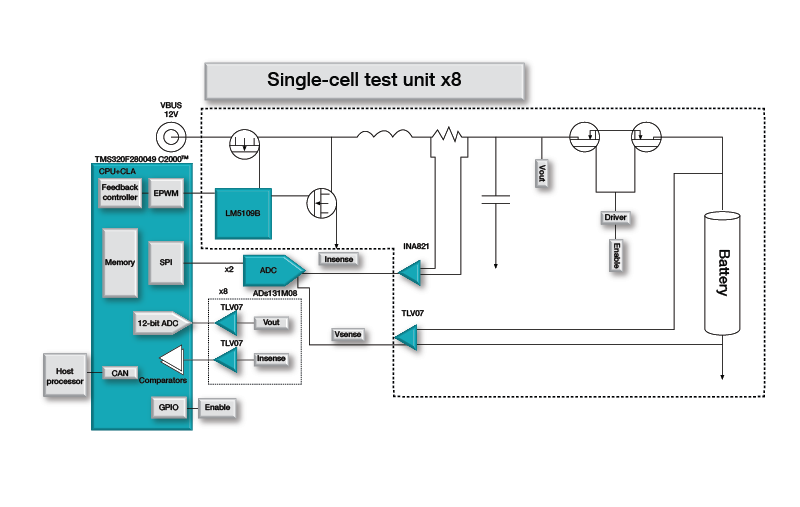
Figure 3 is a block diagram of the reference design. The TMS320F280049 MCU can control up to 8 independent channels. It generates a high-resolution 16-bit PWM for a synchronous buck power stage and performs subroutines for current and voltage control loops. The INA821 instrumentation amplifier senses the current and the TLV07 operational amplifier senses the voltage. Current and voltage signals are converted to digital data by both the external ADS131M08 ADC and the C2000 on-chip ADC. Having the 16-bit ADC in the feedback achieves a control accuracy better than ±0.01%. For cost-optimized systems, you can eliminate the ADS131M08 from the feedback and use the on-chip 12-bit ADC instead to achieve a control accuracy less than ±0.05%
Implementing a multifeedback controller achieves a smooth constant-current to constant-voltage transition where the inner loop is always in constant-current mode. Upon the detection of a constant-voltage-mode condition, the constant-voltage loop output connects to the constant-current loop.
 Figure 3 Digital control loop battery tester
Conclusion
A digital architecture makes it possible to address high accuracy, high current, speed and flexibility without heavy capital investments in battery testing equipment. Rather than investing in multiple architectures for different current levels, you can now test a range of currents so that your high-current equipment no longer remains idle when testing low-current applications.
TI’s digital control reference design enables you to save overall system costs by investing in lower-current battery testing equipment, providing the capabilities and flexibility to test multiple current ranges without sacrificing accuracy.
IMPORTANT NOTICE AND DISCLAIMER
TI PROVIDES TECHNICAL AND RELIABILITY DATA (INCLUDING DATASHEETS), DESIGN RESOURCES (INCLUDING REFERENCE DESIGNS), APPLICATION OR OTHER DESIGN ADVICE, WEB TOOLS, SAFETY INFORMATION, AND OTHER RESOURCES “AS IS” AND WITH ALL FAULTS, AND DISCLAIMS ALL WARRANTIES, EXPRESS AND IMPLIED, INCLUDING WITHOUT LIMITATION ANY IMPLIED WARRANTIES OF MERCHANTABILITY, FITNESS FOR A PARTICULAR PURPOSE OR NON-INFRINGEMENT OF THIRD PARTY INTELLECTUAL PROPERTY RIGHTS.
These resources are intended for skilled developers designing with TI products. You are solely responsible for (1) selecting the appropriate TI products for your application, (2) designing, validating and testing your application, and (3) ensuring your application meets applicable standards, and any other safety, security, or other requirements. These resources are subject to change without notice. TI grants you permission to use these resources only for development of an application that uses the TI products described in the resource. Other reproduction and display of these resources is prohibited. No license is granted to any other TI intellectual property right or to any third party intellectual property right. TI disclaims responsibility for, and you will fully indemnify TI and its representatives against, any claims, damages, costs, losses, and liabilities arising out of your use of these resources.
TI’s products are provided subject to TI’s Terms of Sale (www.ti.com/legal/termsofsale.html) or other applicable terms available either on ti.com or provided in conjunction with such TI products. TI’s provision of these resources does not expand or otherwise alter TI’s applicable warranties or warranty disclaimers for TI products.
Mailing Address: Texas Instruments, Post Office Box 655303, Dallas, Texas 75265
Copyright © 2023, Texas Instruments Incorporated