-
Dimming in Switched-mode LED Drivers
Dimming in Switched-mode LED Drivers
Issac Hsu
One of the key concerns in light-emitting diode (LED) driver designs is the dimming performance. Most designers use one of two methods: analog dimming or digital pulse-width modulation (PWM) dimming. There are two ways to implement digital PWM dimming: an enabling on/off approach or a shunt-field effect transistor (FET) approach. In both implementations, the LEDs will turn on or off according to the duty cycle of the digital PWM signal; yet the responses of the LED drivers are different. In this post, I will review the implementation and advantages of each dimming method.
Analog dimming uses a proportional input voltage to make a linear adjustment of the LED output current level. Many devices, like TI’s TPS92515 or LM3409 LED drivers, have a dedicated analog dimming pin with which to adjust the internal sense voltage. Alternatively, for applications with a microcontroller (MCU), the TPS92518 uses the Serial Peripheral Interface (SPI) communications interface to digitally program two internal registers to analog-dim two independent LED channels.
The drawback of analog dimming is that the current output is not linearly related to the input voltage when the required output current becomes small, due to the offset voltage of the internal operational amplifier. For example, if the LED driver’s internal operation amplifier offset voltage is ±5mV, when the sense voltage is 200mV the error of the regulated current will be 5mV/200mV = ±2.5%. When the sense voltage is 20mV, the error of the regulated current will be 5mV/20mV = 25%.
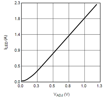
Although it is possible to use analog dimming outside the linear range, some designers prefer to stay in the linear range given the simplicity of the linear relationship. An example of analog dimming linearity is shown in Figure 1.
 Figure 1 An Example of Analog Dimming
Control (from the LM3409 Data Sheet)
Figure 1 An Example of Analog Dimming
Control (from the LM3409 Data Sheet)Digital PWM dimming methods typically can achieve much wider linear dimming ranges than analog dimming, which is good for low brightness dimming. In the digital PWM dimming enabling on/off approach, the LED driver turns on or off according to the duty cycle of the input PWM signal, which comes from an MCU or other external source. The main delay in PWM dimming comes from turning the output drive on and off, and the subsequent ramping up and down of the inductor current. If the LED driver has a low closed-loop bandwidth, the response to the PWM signal is intrinsically slow and cannot easily achieve low brightness.
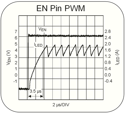
Let’s say that an LED driver runs at a 1MHz switching frequency, with its bandwidth tuned so that the output current settles within five cycles. In this case, 5µs will be the minimum turn-on time for the LED driver to provide a stable light output. If the input PWM dimming signal is 200Hz, then the period will be 5ms. In order to maintain a minimum 5µs turn-on time, the dimming ratio will be 5ms to 5µs, or 1,000-to-1. In other words, the minimum PWM dimming duty cycle will be 0.1% at a 200Hz PWM dimming frequency running at a 1MHz switching frequency. Figure 2 shows the delay of the LED current in a typical enabling on/off approach PWM dimming scenario.
 Figure 2 Digital PWM Dimming Enabling
On/off Approach
Figure 2 Digital PWM Dimming Enabling
On/off ApproachTo further improve the dimming performance, you could either optimize the loop bandwidth to shrink the settling time or set the LED driver to run at a higher switching frequency. The TPS92518 has two independent PWM input pins to control the brightness of the two LED channels.
Shunt-FET PWM dimming is an alternative approach that leaves the LED driver turned on. The digital PWM signal controls a shunt-FET connected to the LED load in parallel to redirect the output current flowing away from the LED through and into the shunt-FET according to the inverse of the duty cycle of the PWM signal. It’s best not to use this approach with LED drivers that require huge output capacitors because the output capacitor stored energy that might introduce high current overshoot, damaging either the shunt-FET or the LED load.
This makes LED drivers with a hysteretic control architecture such as the TPS92518 a good fit for shunt FET dimming. Hysteretic-type LED drivers are open loop, and therefore do not have the loop-bandwidth limitations of closed-loop switching-type LED drivers. The benefit of shunt-FET dimming, with a well-controlled inductor current band, is extremely fast LED turn-on or turn-off times (within nanoseconds), which enable low brightness through a low-duty-cycle PWM signal. Figure 3 shows the delay of the LED current being very small in shunt-FET PWM dimming scenario.
 Figure 3 Shunt-FET PWM Dimming
More and more applications require an MCU to communicate with LED drivers for brightness control. The TPS92518 has an SPI control interface to set the LED current level through an 8-bit digital byte, enabling you to adjust the LED current on the fly. The SPI control interface sets the nominal running off-time digitally instead of using a resistor-capacitor circuit on the off-time control pin. TPS92518 has another register programmed through SPI to set the maximum off-time to realize the well-controlled inductor current band during shunt-FET PWM dimming.
The TPS92518 has an internal ADC to convert the output voltages of both channels and estimated die temperature into digital code. This information is stored in the register of TPS92518 and available for read-back through the SPI interface. The architecture of the TPS92518 allows either enabling on/off PWM dimming or shunt-FET PWM dimming.
You will have to choose between analog dimming and PWM dimming to control LED brightness based on your design’s requirements. The analog dimming method does not require a digital signal input; however, deep dimming is not readily available with this method. Both implementations of the PWM dimming method can achieve a much higher dimming ratio, but require more effort to design properly.
Additional Resources
- Watch these TI Training videos:
IMPORTANT NOTICE AND DISCLAIMER
TI PROVIDES TECHNICAL AND RELIABILITY DATA (INCLUDING DATASHEETS), DESIGN RESOURCES (INCLUDING REFERENCE DESIGNS), APPLICATION OR OTHER DESIGN ADVICE, WEB TOOLS, SAFETY INFORMATION, AND OTHER RESOURCES “AS IS” AND WITH ALL FAULTS, AND DISCLAIMS ALL WARRANTIES, EXPRESS AND IMPLIED, INCLUDING WITHOUT LIMITATION ANY IMPLIED WARRANTIES OF MERCHANTABILITY, FITNESS FOR A PARTICULAR PURPOSE OR NON-INFRINGEMENT OF THIRD PARTY INTELLECTUAL PROPERTY RIGHTS.
These resources are intended for skilled developers designing with TI products. You are solely responsible for (1) selecting the appropriate TI products for your application, (2) designing, validating and testing your application, and (3) ensuring your application meets applicable standards, and any other safety, security, or other requirements. These resources are subject to change without notice. TI grants you permission to use these resources only for development of an application that uses the TI products described in the resource. Other reproduction and display of these resources is prohibited. No license is granted to any other TI intellectual property right or to any third party intellectual property right. TI disclaims responsibility for, and you will fully indemnify TI and its representatives against, any claims, damages, costs, losses, and liabilities arising out of your use of these resources.
TI’s products are provided subject to TI’s Terms of Sale (www.ti.com/legal/termsofsale.html) or other applicable terms available either on ti.com or provided in conjunction with such TI products. TI’s provision of these resources does not expand or otherwise alter TI’s applicable warranties or warranty disclaimers for TI products.
Mailing Address: Texas Instruments, Post Office Box 655303, Dallas, Texas 75265
Copyright © 2023, Texas Instruments Incorporated