-
Quick Fixes to Common I2C Headaches
Quick Fixes to Common I2C Headaches
Kaitlyn Mazzarella
If you’ve ever programmed anything in your life, you know the feeling of relief that comes with writing your code and having it work with no errors on your first try. Back in the days of Computer Science 101, this was much more feasible. Unfortunately, it rarely happens in the real world, although trial and error can sometimes be how we learn.
Take designing an Inter-Integrated Circuit (I2C) bus, for example. Many designers use I2C for its simplicity – however, the specification is still 64 pages of rules on how to communicate with the protocol. When your first printed circuit board (PCB) comes back and your I2C bus isn’t communicating properly, you’re in for a long night and a huge headache. So in this post, I’ll identify two very common I2C bus problems and introduce solutions to address them.
Headache No. 1: Static Voltage Offset Mismatch
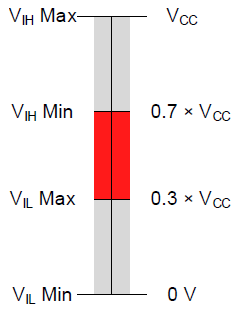
I2C slave devices send a signal to the I2C master when they have data to transmit, and they do this by pulling the bus to a low state. A common headache with I2C bus design is when the output low voltage (VOL) of one device is not low enough to meet the threshold of another device’s input low voltage (VIL) requirement. The I2C standard states that a “low” is 30% of the VCC value, and anything above 70% of VCC is a “high.” This leaves an undefined region between the two thresholds, as shown in Figure 1.
 Figure 1 I2C Voltage-level Thresholds
Ideally, your VOL spec should be as close to 0V as possible, in order to eliminate any potential to hit the undefined range after considering other parasitics such as series resistance or high current loads. Previously, most I2C devices (such as the TCA9517) had a static voltage offset, which results in a VOL of ~0.5V. However, TI has developed a new architecture that eliminates the requirement for a static voltage offset, resulting in a VOL of ~0.2V for the TCA9802, one variant of this new family of TCA980x products.
Headache No. 2: Rise-time Violations
One benefit of I2C is that it can communicate with multiple devices on the same bus, as long as you limit the capacitance to 400pF. However, additional considerations come into play here as well. Headache No. 2 is often associated with rise-time issues caused by systems with complex I2C buses, either caused by having many devices on the bus or long board traces. This type of heavily loaded bus will result in large capacitance with traditional I2C buffer devices, which will in turn slow down the rising edge of your signal. The new series of I2C buffer devices uses an integrated current source to drive the bus, rather than pull-up resistor-based devices (shown in Figure 2).
 Figure 2 Architecture of a Traditional I2C Buffer (a) vs. the TCA980x Buffer (b)
This constant current drive enables a quicker rise time and a more controlled falling edge, resulting in much stronger signal integrity, as shown in Figure 3. The light blue signal in Figure 3 shows the new current source-based architecture compared with a competitor solution shown in dark blue. This new architecture helps prevent ringing on the falling edge, which will also prevent noise reflections on the bus.
 Figure 3 TCA980x Rise-time Benefit vs. the Competition
TI’s new architecture takes these common design headaches into consideration and provides simple solutions to prevent them. I2C is a standard that intends to simplify designs, which is exactly what the new TCA980x family helps do.
For more details about solving problems with this device family, read the application report, “Advantages and Design Considerations of the TCA980x Family” or see the full portfolio.
Additional Resources
- Learn more about TI’s portfolio of I2C buffered translators, I/O expanders and switches.
- Find the right device for your application with the application report, “Choosing the Correct I2C Device for New Designs.”
- Watch this video which provides additional details about the the TCA980x family benefits.
IMPORTANT NOTICE AND DISCLAIMER
TI PROVIDES TECHNICAL AND RELIABILITY DATA (INCLUDING DATASHEETS), DESIGN RESOURCES (INCLUDING REFERENCE DESIGNS), APPLICATION OR OTHER DESIGN ADVICE, WEB TOOLS, SAFETY INFORMATION, AND OTHER RESOURCES “AS IS” AND WITH ALL FAULTS, AND DISCLAIMS ALL WARRANTIES, EXPRESS AND IMPLIED, INCLUDING WITHOUT LIMITATION ANY IMPLIED WARRANTIES OF MERCHANTABILITY, FITNESS FOR A PARTICULAR PURPOSE OR NON-INFRINGEMENT OF THIRD PARTY INTELLECTUAL PROPERTY RIGHTS.
These resources are intended for skilled developers designing with TI products. You are solely responsible for (1) selecting the appropriate TI products for your application, (2) designing, validating and testing your application, and (3) ensuring your application meets applicable standards, and any other safety, security, or other requirements. These resources are subject to change without notice. TI grants you permission to use these resources only for development of an application that uses the TI products described in the resource. Other reproduction and display of these resources is prohibited. No license is granted to any other TI intellectual property right or to any third party intellectual property right. TI disclaims responsibility for, and you will fully indemnify TI and its representatives against, any claims, damages, costs, losses, and liabilities arising out of your use of these resources.
TI’s products are provided subject to TI’s Terms of Sale (www.ti.com/legal/termsofsale.html) or other applicable terms available either on ti.com or provided in conjunction with such TI products. TI’s provision of these resources does not expand or otherwise alter TI’s applicable warranties or warranty disclaimers for TI products.
Mailing Address: Texas Instruments, Post Office Box 655303, Dallas, Texas 75265
Copyright © 2023, Texas Instruments Incorporated