-
How to Achieve Higher System Efficiency- Part Two: High-speed Gate Drivers
How to Achieve Higher System Efficiency- Part Two: High-speed Gate Drivers
It’s the new year and designers are still pursuing higher efficiency in their designs. In part one of this series, I discussed how high-current gate drivers can help systems achieve higher efficiency. High-speed gate drivers can accomplish the same.
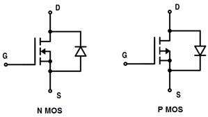
A high-speed gate driver can increase efficiencies by reducing the power consumed from a FET’s body diode. A body diode is a parasitic diode, intrinsic to most types of FETs. It is formed by the p-n junction and sits between the drain and source. Figure 1 shows the body diode represented in a typical MOSFET circuit symbol.
 Figure 1 MOSFET Symbols Including
Intrinsic Body Diode
Figure 1 MOSFET Symbols Including
Intrinsic Body DiodeLimiting the conduction time of the body diode will in turn reduce the power consumed across it. This is because the voltage drop across the body diode is typically higher than the voltage across the MOSFET when the MOSFET is in the on state. Since P = I x V (where P is power consumed, I is current, and V is the voltage drop) for the same current levels, the conduction losses through the MOSFET channel are significantly lower than through the body diode.
These concepts come into play in synchronous rectification of power electronic circuits. Synchronous rectification improves the efficiency of these circuits by replacing the diodes with an actively controlled device such as a power MOSFET. Reducing body-diode conduction maximizes the benefits of this technique.
Let’s consider a synchronous buck converter. The body diode of the low-side FET becomes forward-biased when the high-side FET turns off and there is still current in the inductor. After a small dead time, which is necessary to avoid shoot-through, the low-side FET turns on and starts conducting through its channel. The same principles apply to other synchronous half-bridge configurations, typically found in DC/DC power supplies and motor-drive designs.
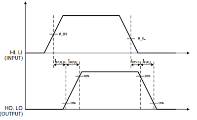
An important gate-driver parameter responsible for high-speed turn-on is the turn-on propagation delay. This is the time between when a signal is applied at the input of the gate driver to the time that the output starts to go high. An example of this is shown in Figure 2. The idea is that as the FET switches back on, the body diode will switch off. Fast turn-on propagation delays enable quicker switching on of a FET, minimizing the conduction time of the body diode and thus minimizing losses.
 Figure 2 Timing Diagram Where t_PDLH
Represents the Turn-on Propagation Delay
Figure 2 Timing Diagram Where t_PDLH
Represents the Turn-on Propagation DelayTI’s portfolio includes gate drivers with industry-leading high-speed turn-on propagation delays. See Table 1.
| Category | Device | Description | Turn-on propagation delay |
|---|---|---|---|
| High-speed drivers | UCC27517A | 4A/4A high-speed low-side gate driver | 13ns |
| UCC27611 | 4A/6A high-speed low-side gate driver | 14ns | |
| UCC27201A | 3A, 120V high- and low-side driver | 20ns |
System efficiency is a team effort. This blog series illustrates how both high speed and high current gate drivers are key pieces. Start designing your high-efficiency system today by visiting www.ti.com/gatedrivers.
Additional Resources
- This reference design in the TI Designs library showcases high-speed gate drivers in high-efficiency systems:
IMPORTANT NOTICE AND DISCLAIMER
TI PROVIDES TECHNICAL AND RELIABILITY DATA (INCLUDING DATASHEETS), DESIGN RESOURCES (INCLUDING REFERENCE DESIGNS), APPLICATION OR OTHER DESIGN ADVICE, WEB TOOLS, SAFETY INFORMATION, AND OTHER RESOURCES “AS IS” AND WITH ALL FAULTS, AND DISCLAIMS ALL WARRANTIES, EXPRESS AND IMPLIED, INCLUDING WITHOUT LIMITATION ANY IMPLIED WARRANTIES OF MERCHANTABILITY, FITNESS FOR A PARTICULAR PURPOSE OR NON-INFRINGEMENT OF THIRD PARTY INTELLECTUAL PROPERTY RIGHTS.
These resources are intended for skilled developers designing with TI products. You are solely responsible for (1) selecting the appropriate TI products for your application, (2) designing, validating and testing your application, and (3) ensuring your application meets applicable standards, and any other safety, security, or other requirements. These resources are subject to change without notice. TI grants you permission to use these resources only for development of an application that uses the TI products described in the resource. Other reproduction and display of these resources is prohibited. No license is granted to any other TI intellectual property right or to any third party intellectual property right. TI disclaims responsibility for, and you will fully indemnify TI and its representatives against, any claims, damages, costs, losses, and liabilities arising out of your use of these resources.
TI’s products are provided subject to TI’s Terms of Sale (www.ti.com/legal/termsofsale.html) or other applicable terms available either on ti.com or provided in conjunction with such TI products. TI’s provision of these resources does not expand or otherwise alter TI’s applicable warranties or warranty disclaimers for TI products.
Mailing Address: Texas Instruments, Post Office Box 655303, Dallas, Texas 75265
Copyright © 2023, Texas Instruments Incorporated